BeMicro Max 10
Success! Subscription added.
Success! Subscription removed.
Sorry, you must verify to complete this action. Please click the verification link in your email. You may re-send via your profile.
BeMicro Max 10
- Subscribe to RSS Feed
- Mark as New
- Mark as Read
- Bookmark
- Subscribe
- Printer Friendly Page
- Report Inappropriate Content
BeMicro Max 10
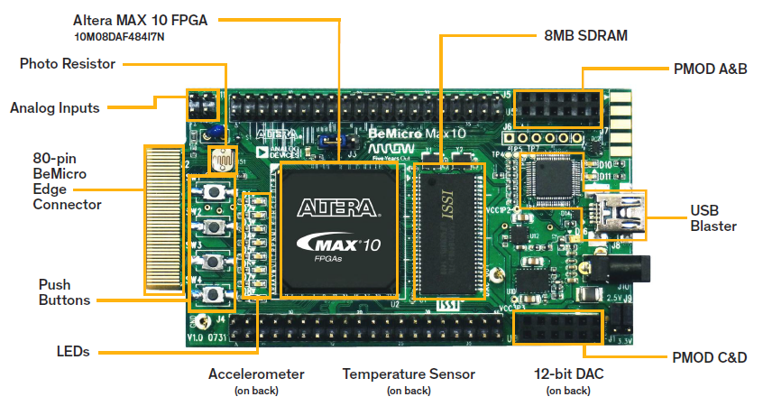
BeMicro Max 10 FPGA Evaluation Kit
BeMicro Max 10 is an FPGA Evalution Kit produced by Arrow Electronics. It is available at http://www.arrow.com/bemicro/
BeMicro Max 10 adopts Altera’s non-volatile MAX 10 FPGA built on 55-nm flash process. Users can take advantage of the features Altera offers in the MAX 10 FPGA device, such as an ADC block, temperature sense diode and flash memory. BeMicro Max 10 includes a variety of peripherals connected to the MAX 10 FPGA such as 8MB SDRAM, accelerometer, digital-to-analog converter (DAC), temperature sensor, thermal resistor, photo resistor, LEDs, pushbuttons and several different options for expansion connectivity.
Board Highlights
Features Altera MAX 10 FPGA with ADC block, temperature sense diode, onchip-RAM, user flash memory and non-volatile self-configuration.
- Extensible via 2 Digital PMOD Interface headers
- Allows for further expansion from two 40-pin prototyping headers
- 3-Axis MEMS Accelerometer from Analog Devices (ADXL362)
- 12-bit Digital-to-Analog Converter from Analog Devices (AD5681R)
- Digital Temperature Sensor from Analog Devices (ADT7420)
- 8 MB SDRAM
- One MAX 10 FPGA (10M08DAF484xxx)
- 8,000 LEs
- 414 Kbit (Kb) M9K memory
- 256 Kbit (Kb) user flash memory
- 2 phase locked loops (PLLs)
- 24 18x18-bit multipliers
- 1 ADC block – 1 MSa/sec, 12-bit, 18-channels
- 17 analog inputs
- 1 temperature sense diode
- 250 general purpose input/output (GPIO)
- Non-volatile self-configuration with dual-boot support
- Embedded USB-Blaster™ for use with the Quartus® II Programmer. This USB-Blaster can be used to program external Altera-devices as well.
- Note that this board is shipping with an ES (Engineering Silicon) part
Documentation
- BeMicro Max 10 Getting Started User Guide (PDF)
- BeMicro Max 10 BOM (ZIP)
- BeMicro Max 10 Schematic (PDF)
Errata
ADC Offset Issue
When reading the MAX®10 ADC channels on the BeMicro Max 10 the value that is read by the ADC differs from what is measured using an external oscilloscope. This constant offset reading occurs because there is an incorrect voltage connection on I/O Banks VCCIO1A and VCCIO1B (originally set to 3.3V).
To correct this issue, VCCIO1A and VCCIO1B need to be connected to a 2.5V rail for this dual-supply device.
Tutorial Labs
Intro to FPGA Simple Tutorial
Intro to FPGA Simple PWM Tutorial
ADC Finger Temperature (fingertemp) Tutorial
- BeMicro Max 10 ADC Finger Temperature Tutorial (PDF)
- Fingertemp Lab Files (QAR)
- Fingertemp Lab Files Complete(don't cheat!) (QAR)
VGA Tutorial
Simple Nios II Tutorial
Dual Boot Tutorial
Embedded Systems Lab
This is a full day lab in which the user will build a complete Nios II processor based system using the QSys system integration tool.
Note: you may need to modify the bemicro_max10_serial_flash_controller_hw.tcl in the IP directory for Quartus 15.0 and later Line 20 calling out supported devices, change MAX10FPGA to MAX10 (this will be needed for Quartus 15.0 and later) without this change, the IP will be grayed out in Qsys.
LVDS Loopback Tutorial
Example Designs
Example designs are now being supported in Altera's Design Store. The links below for the project archive will take you to the latest version on the Altera design store.
Empty Baseline Project (starting point for your own design)
WARNING: There is a pin assignment error in the template project below. The following pin pairs on J4 are swapped: 11/12, 13/14, 15/16, 17/18, 19/20, 21/22, 23/24, 25/26, 27/28, 29/30, 31/32, 33/34, 35/36, 37/38, 39/40.
- BeMicro Max 10 empty Quartus project with pin assignments and empty top level Verilog or VHDL file (Design Store link)
- Documentation Describing the Empty Baseline Project (PDF)
- BeMicro Max 10 System Builder Verilog (Working)
Full featured Reference Design
- BeMicro Max 10 reference design containing interfaces to the DAC, ADC, Temperature Sensor, Accelerometer, and Photo Sensor (Design Store link)
- User Guide Explaining How To Get Started with the Full Featured Reference Design (PDF)
DC-DC Converter Control with ADSP Builder
Low Level C Programming with BeMicro board
Community support is provided during standard business hours (Monday to Friday 7AM - 5PM PST). Other contact methods are available here.
Intel does not verify all solutions, including but not limited to any file transfers that may appear in this community. Accordingly, Intel disclaims all express and implied warranties, including without limitation, the implied warranties of merchantability, fitness for a particular purpose, and non-infringement, as well as any warranty arising from course of performance, course of dealing, or usage in trade.
For more complete information about compiler optimizations, see our Optimization Notice.
