- Mark as New
- Bookmark
- Subscribe
- Mute
- Subscribe to RSS Feed
- Permalink
- Report Inappropriate Content
When creating a new Quartus project similar to a demo example, I am trying to place XCVR pins in a blank project and getting an error from the 1.5V PMCL differential pins (HSMC_GXB_RX_p0 and HSMC_GXB_TX_p0 for example).
Why am I getting this fitter error and do I need some minimum of connections to support the differential pins, and if that is the case what is the minimum code I need to declare these pins in a new project so it compiles?
I believe I have the IO standard correctly set to 1.5V PCML and Pins set to the recommended pins in the User's Guide and there are no other pins conflicting that I can see in the QSF file.
Compiler Error:
Error (14566): The Fitter cannot place 2 periphery component(s) due to conflicts with existing constraints (2 pin(s)). Fix the errors described in the submessages, and then rerun the Fitter. The Intel FPGA Knowledge Database may also contain articles with information on how to resolve this periphery placement failure. Review the errors and then visit the Knowledge Database at https://www.altera.com/support/support-resources/knowledge-base/search.html and search for this specific error message number.
Error (175020): The Fitter cannot place logic pin in region (0, 11) to (0, 11), to which it is constrained, because there are no valid locations in the region for logic of this type.
Info (14596): Information about the failing component(s):
Info (175028): The pin name(s): HSMC_GXB_TX_p0
Error (16234): No legal location could be found out of 1 considered location(s). Reasons why each location could not be used are summarized below:
Error (184016): There were not enough differential output pin locations available (1 location affected)
Info (175029): pin containing PIN_AE4
Info (175015): The I/O pad HSMC_GXB_TX_p0 is constrained to the location PIN_AE4 due to: User Location Constraints (PIN_AE4)
Info (14709): The constrained I/O pad is contained within this pin
Error (175020): The Fitter cannot place logic pin in region (0, 14) to (0, 14), to which it is constrained, because there are no valid locations in the region for logic of this type.
Info (14596): Information about the failing component(s):
Info (175028): The pin name(s): HSMC_GXB_RX_p0
Error (16234): No legal location could be found out of 1 considered location(s). Reasons why each location could not be used are summarized below:
Error (184016): There were not enough differential input pin locations available (1 location affected)
Info (175029): pin containing PIN_AD2
Info (175015): The I/O pad HSMC_GXB_RX_p0 is constrained to the location PIN_AD2 due to: User Location Constraints (PIN_AD2)
Info (14709): The constrained I/O pad is contained within this pin
.QSF file output:
set_global_assignment -name FAMILY "Cyclone V"
set_global_assignment -name DEVICE 5CGXFC5C6F27C7
set_global_assignment -name TOP_LEVEL_ENTITY CPL_HDL
set_global_assignment -name ORIGINAL_QUARTUS_VERSION 16.1.0
set_global_assignment -name PROJECT_CREATION_TIME_DATE "19:00:27 JUNE 13, 2022"
set_global_assignment -name LAST_QUARTUS_VERSION "16.1.0 Lite Edition"
set_global_assignment -name PROJECT_OUTPUT_DIRECTORY output_files
set_global_assignment -name MIN_CORE_JUNCTION_TEMP 0
set_global_assignment -name MAX_CORE_JUNCTION_TEMP 85
set_global_assignment -name ERROR_CHECK_FREQUENCY_DIVISOR 256
set_global_assignment -name EDA_SIMULATION_TOOL "ModelSim (Verilog)"
set_global_assignment -name EDA_TIME_SCALE "1 ps" -section_id eda_simulation
set_global_assignment -name EDA_OUTPUT_DATA_FORMAT "VERILOG HDL" -section_id eda_simulation
set_global_assignment -name VERILOG_FILE CPL_HDL.v
set_global_assignment -name PARTITION_NETLIST_TYPE SOURCE -section_id Top
set_global_assignment -name PARTITION_FITTER_PRESERVATION_LEVEL PLACEMENT_AND_ROUTING -section_id Top
set_global_assignment -name PARTITION_COLOR 16764057 -section_id Top
set_global_assignment -name RELEASE_CLEARS_BEFORE_TRI_STATES ON
set_global_assignment -name ENABLE_OCT_DONE OFF
set_global_assignment -name ENABLE_CONFIGURATION_PINS OFF
set_global_assignment -name ENABLE_BOOT_SEL_PIN OFF
set_global_assignment -name STRATIXV_CONFIGURATION_SCHEME "PASSIVE SERIAL"
set_global_assignment -name USE_CONFIGURATION_DEVICE ON
set_global_assignment -name CRC_ERROR_OPEN_DRAIN ON
set_global_assignment -name OUTPUT_IO_TIMING_NEAR_END_VMEAS "HALF VCCIO" -rise
set_global_assignment -name OUTPUT_IO_TIMING_NEAR_END_VMEAS "HALF VCCIO" -fall
set_global_assignment -name OUTPUT_IO_TIMING_FAR_END_VMEAS "HALF SIGNAL SWING" -rise
set_global_assignment -name OUTPUT_IO_TIMING_FAR_END_VMEAS "HALF SIGNAL SWING" -fall
set_global_assignment -name ACTIVE_SERIAL_CLOCK FREQ_100MHZ
set_global_assignment -name POWER_PRESET_COOLING_SOLUTION "23 MM HEAT SINK WITH 200 LFPM AIRFLOW"
set_global_assignment -name POWER_BOARD_THERMAL_MODEL "NONE (CONSERVATIVE)"
set_global_assignment -name TIMEQUEST_MULTICORNER_ANALYSIS ON
set_global_assignment -name NUM_PARALLEL_PROCESSORS ALL
set_instance_assignment -name IO_STANDARD "1.5-V PCML" -to HSMC_GXB_RX_p0
set_location_assignment PIN_AD2 -to HSMC_GXB_RX_p0
set_location_assignment PIN_AD1 -to "HSMC_GXB_RX_p0(n)"
set_instance_assignment -name IO_STANDARD "1.5-V PCML" -to HSMC_GXB_TX_p0
set_instance_assignment -name IO_STANDARD "1.2 V" -to ADC_CONVST
set_location_assignment PIN_AB22 -to ADC_CONVST
set_location_assignment PIN_AA21 -to ADC_SCK
set_instance_assignment -name IO_STANDARD "1.2 V" -to ADC_SCK
set_location_assignment PIN_Y10 -to ADC_SDI
set_location_assignment PIN_W10 -to ADC_SDO
set_instance_assignment -name IO_STANDARD "1.2 V" -to ADC_SDI
set_instance_assignment -name IO_STANDARD "1.2 V" -to ADC_SDO
set_location_assignment PIN_D7 -to AUD_ADCDAT
set_location_assignment PIN_C7 -to AUD_ADCLRCK
set_location_assignment PIN_E6 -to AUD_BCLK
set_location_assignment PIN_H10 -to AUD_DACDAT
set_location_assignment PIN_G10 -to AUD_DACLRCK
set_location_assignment PIN_D6 -to AUD_XCK
set_location_assignment PIN_R20 -to CLOCK_50_B5B
set_instance_assignment -name IO_STANDARD "2.5 V" -to AUD_ADCDAT
set_instance_assignment -name IO_STANDARD "2.5 V" -to AUD_ADCLRCK
set_instance_assignment -name IO_STANDARD "2.5 V" -to AUD_BCLK
set_instance_assignment -name IO_STANDARD "2.5 V" -to AUD_DACDAT
set_instance_assignment -name IO_STANDARD "2.5 V" -to AUD_DACLRCK
set_instance_assignment -name IO_STANDARD "2.5 V" -to AUD_XCK
set_instance_assignment -name IO_STANDARD "3.3-V LVTTL" -to CLOCK_50_B5B
set_location_assignment PIN_N20 -to CLOCK_50_B6A
set_location_assignment PIN_H12 -to CLOCK_50_B7A
set_instance_assignment -name IO_STANDARD "3.3-V LVTTL" -to CLOCK_50_B6A
set_instance_assignment -name IO_STANDARD "2.5 V" -to CLOCK_50_B7A
set_location_assignment PIN_M10 -to CLOCK_50_B8A
set_instance_assignment -name IO_STANDARD "2.5 V" -to CLOCK_50_B8A
set_location_assignment PIN_U12 -to CLOCK_125_p
set_instance_assignment -name IO_STANDARD LVDS -to CLOCK_125_p
set_location_assignment PIN_V12 -to "CLOCK_125_p(n)"
set_global_assignment -name FLOW_DISABLE_ASSEMBLER OFF
set_location_assignment PIN_AE4 -to HSMC_GXB_TX_p0
set_location_assignment PIN_AE3 -to "HSMC_GXB_TX_p0(n)"
set_global_assignment -name SMART_RECOMPILE OFF
set_location_assignment PIN_AB24 -to CPU_RESET_n
set_location_assignment PIN_Y18 -to HEX0[6]
set_location_assignment PIN_Y19 -to HEX0[5]
set_location_assignment PIN_Y20 -to HEX0[4]
set_location_assignment PIN_W18 -to HEX0[3]
set_location_assignment PIN_V19 -to HEX0[0]
set_location_assignment PIN_V18 -to HEX0[1]
set_location_assignment PIN_V17 -to HEX0[2]
set_location_assignment PIN_AA18 -to HEX1[0]
set_location_assignment PIN_AD26 -to HEX1[1]
set_location_assignment PIN_AB19 -to HEX1[2]
set_location_assignment PIN_AE26 -to HEX1[3]
set_location_assignment PIN_AE25 -to HEX1[4]
set_location_assignment PIN_AC19 -to HEX1[5]
set_location_assignment PIN_AF24 -to HEX1[6]
set_instance_assignment -name IO_STANDARD "1.2 V" -to HEX0[0]
set_instance_assignment -name IO_STANDARD "1.2 V" -to HEX0[1]
set_instance_assignment -name IO_STANDARD "1.2 V" -to HEX0[2]
set_instance_assignment -name IO_STANDARD "1.2 V" -to HEX0[3]
set_instance_assignment -name IO_STANDARD "1.2 V" -to HEX0[4]
set_instance_assignment -name IO_STANDARD "1.2 V" -to HEX0[5]
set_instance_assignment -name IO_STANDARD "1.2 V" -to HEX0[6]
set_instance_assignment -name IO_STANDARD "1.2 V" -to HEX1[0]
set_instance_assignment -name IO_STANDARD "1.2 V" -to HEX1[1]
set_instance_assignment -name IO_STANDARD "1.2 V" -to HEX1[2]
set_instance_assignment -name IO_STANDARD "1.2 V" -to HEX1[3]
set_instance_assignment -name IO_STANDARD "1.2 V" -to HEX1[4]
set_instance_assignment -name IO_STANDARD "1.2 V" -to HEX1[5]
set_instance_assignment -name IO_STANDARD "1.2 V" -to HEX1[6]
set_instance_assignment -name IO_STANDARD "3.3-V LVTTL" -to CPU_RESET_n
set_location_assignment PIN_B7 -to I2C_SCL
set_location_assignment PIN_G11 -to I2C_SDA
set_instance_assignment -name IO_STANDARD "2.5 V" -to I2C_SCL
set_instance_assignment -name IO_STANDARD "2.5 V" -to I2C_SDA
set_location_assignment PIN_P11 -to KEY[0]
set_location_assignment PIN_P12 -to KEY[1]
set_location_assignment PIN_Y15 -to KEY[2]
set_location_assignment PIN_Y16 -to KEY[3]
set_instance_assignment -name IO_STANDARD "1.2 V" -to KEY[3]
set_instance_assignment -name IO_STANDARD "1.2 V" -to KEY[2]
set_instance_assignment -name IO_STANDARD "1.2 V" -to KEY[1]
set_instance_assignment -name IO_STANDARD "1.2 V" -to KEY[0]
set_instance_assignment -name PARTITION_HIERARCHY root_partition -to | -section_id Top
- Mark as New
- Bookmark
- Subscribe
- Mute
- Subscribe to RSS Feed
- Permalink
- Report Inappropriate Content
Hi Terra,
I have told you earlier, you cannot directly connect, Please design custom logic to reconstruct the word. First correct your design then try to compile.
Thank you
Kshitij Goel
Link Copied
- Mark as New
- Bookmark
- Subscribe
- Mute
- Subscribe to RSS Feed
- Permalink
- Report Inappropriate Content
Hi Terra,
It is always recommended to instantiate the XCVR. There is article also https://www.intel.com/content/www/us/en/support/programmable/articles/000077932.html
If still you face any issues, please share your project with mentioning the environment details and device details.
Thank you
Kshitij Goel
- Mark as New
- Bookmark
- Subscribe
- Mute
- Subscribe to RSS Feed
- Permalink
- Report Inappropriate Content
Hi, I am using Quartus Prime Lite 16.1 version with a Cyclone V dev board called C5G Starter Kit from Terasic. The exact FPGA device is a Cyclone V 5CGXFC5C6F27C7. I am also using the HSMC (High Density mezzanine connector) to hook up an expansion card. The expansion card has HD-SDI BNC connectors In and Out that are routed through the FPGA.
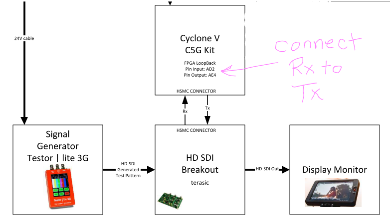
The goal is to short the HSMC_GXB_RX pin to the HSMC_GXB_TX pin in order to make a "straight through" test for the signal. The HD-SDI signal is being generated off the dev boards and, eventually, the FPGA only needs to route the SDI input to one of the two Tx output pairs as a switch.
In Quartus, I cannot find an IP named ALTGXB anywhere in the catalog. On the ALTGXB Intel page it does not say how to install this for a Cyclone V device. Can you help?
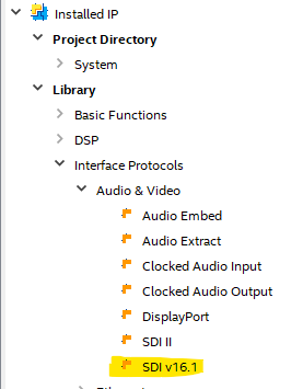
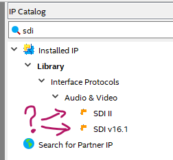
I also searched the IP catalog for XCVR but there is nothing named that. I see SDI v16.1? But these are time sensitive blocks so it may be more fancy than what I need? I am looking for a simple buffer to link the GXB_RX pair to the GXB_Tx pins. Thank you.
-Terra
- Mark as New
- Bookmark
- Subscribe
- Mute
- Subscribe to RSS Feed
- Permalink
- Report Inappropriate Content
Hi,
Can you please share your project.
Thank you
Kshitij Goel
- Mark as New
- Bookmark
- Subscribe
- Mute
- Subscribe to RSS Feed
- Permalink
- Report Inappropriate Content
Hi,
We do not receive any response from you to the previous reply that I have provided. This thread will be transitioned to community support. If you have a new question, feel free to open a new thread to get the support from Intel experts. Otherwise, the community users will continue to help you on this thread.
Thank you
KG
- Mark as New
- Bookmark
- Subscribe
- Mute
- Subscribe to RSS Feed
- Permalink
- Report Inappropriate Content
My project is empty except for pin locations, which file extensions are what you want to see?
I am trying to figure out what is the minimum I need to connect the pins together.
My goal is just to make a straight through connection between these pins:
INPUT: HSMC_GXB_RX[0] on PIN_AD2 (HD-SDI in)
OUTPUT: HSMC_GXB_TX[0] on PIN_AE4 (HD-SDI out)
Any suggestions would be very helpful. I am using the Terasic Developement board C5G with an SDI mezzanine breakout board so I can't really move the pins around too much.
The signal that I am passing through is HD-SDI. (It is NOT a dual link)
- Mark as New
- Bookmark
- Subscribe
- Mute
- Subscribe to RSS Feed
- Permalink
- Report Inappropriate Content
Hi,
Refer to the UG, ALTGXB is transceiver block and which needs to be instantiated.
Thank you
Kshitij Goel
- Mark as New
- Bookmark
- Subscribe
- Mute
- Subscribe to RSS Feed
- Permalink
- Report Inappropriate Content
OK, but do I use SDI II or SDI v16.1?
Also, do I instantiate just one, or do I need a separate one for the RX & TX?
How do I provide the 1.485G Clock?
- Mark as New
- Bookmark
- Subscribe
- Mute
- Subscribe to RSS Feed
- Permalink
- Report Inappropriate Content
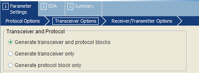
Do I need the protocol blocks for a straight through connection or can I do transceiver only?
- Mark as New
- Bookmark
- Subscribe
- Mute
- Subscribe to RSS Feed
- Permalink
- Report Inappropriate Content
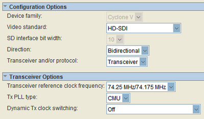
I tried to add SDI_v16.1 as a generate Transceiver only Bidirectional IP Core. Then I added a Altera PLL and created an output clock of 74.25MHz.
I have Quartus setup to add the generated files to the Project automatically, but it doesn't seem to compile.
The Compile errors I am getting now are:
- Info (12021): Found 1 design units, including 1 entities, in source file sdi-library/sdi_rate_detector.v
Info (12023): Found entity 1: sdi_rate_detector
Info (12128): Elaborating entity "sdi_rate_detector" for hierarchy "SDI_v16_t:SDI_v16_Bidirectional1|sdi_megacore_top:sdi_megacore_top_inst|sdi_txrx_port:sdi_txrx_port_gen[0].u_txrx_port|sdi_rate_detector:sdi_receiver_rate_detector.rate_detector_inst"
Error (12006): Node instance "gen_duplex_native.cv_nativephy_inst" instantiates undefined entity "altera_xcvr_native_av". Ensure that required library paths are specified correctly, define the specified entity, or change the instantiation. If this entity represents Intel FPGA or third-party IP, generate the synthesis files for the IP.
Error (12006): Node instance "gen_duplex_native.tx_xcvr_reset_control_inst" instantiates undefined entity "altera_xcvr_reset_control". Ensure that required library paths are specified correctly, define the specified entity, or change the instantiation. If this entity represents Intel FPGA or third-party IP, generate the synthesis files for the IP.
Error (12006): Node instance "gen_duplex_native.rx_xcvr_reset_control_inst" instantiates undefined entity "altera_xcvr_reset_control". Ensure that required library paths are specified correctly, define the specified entity, or change the instantiation. If this entity represents Intel FPGA or third-party IP, generate the synthesis files for the IP.
Error: Quartus Prime Analysis & Synthesis was unsuccessful. 3 errors, 30 warnings
Error: Peak virtual memory: 4795 megabytes
Error: Processing ended: Tue Jul 19 19:00:45 2022
Error: Elapsed time: 00:00:10
Error: Total CPU time (on all processors): 00:00:19
Error (293001): Quartus Prime Full Compilation was unsuccessful. 5 errors, 30 warnings
The code from my top.v file is:
module C5G_HSMC_XCVR_LOOPBACK_TEST(
///////// ADC /////////
output ADC_CONVST,
output ADC_SCK,
output ADC_SDI,
input ADC_SDO,
///////// AUD /////////
input AUD_ADCDAT,
inout AUD_ADCLRCK,
inout AUD_BCLK,
output AUD_DACDAT,
inout AUD_DACLRCK,
output AUD_XCK,
///////// CLOCK /////////
input CLOCK_125_p,
input CLOCK_50_B5B,
input CLOCK_50_B6A,
input CLOCK_50_B7A,
input CLOCK_50_B8A,
///////// CPU /////////
input CPU_RESET_n,
///////// GPIO /////////
inout [35:0] GPIO,
///////// HDMI /////////
output HDMI_TX_CLK,
output [23:0] HDMI_TX_D,
output HDMI_TX_DE,
output HDMI_TX_HS,
input HDMI_TX_INT,
output HDMI_TX_VS,
///////// HEX0 /////////
output [6:0] HEX0,
///////// HEX1 /////////
output [6:0] HEX1,
///////// HSMC /////////
/*
input HSMC_CLKIN0,
input [2:1] HSMC_CLKIN_n,
input [2:1] HSMC_CLKIN_p,
output HSMC_CLKOUT0,
output [2:1] HSMC_CLKOUT_n,
output [2:1] HSMC_CLKOUT_p,
inout [3:0] HSMC_D,
*/
input [0:0] HSMC_GXB_RX_p,
output [0:0] HSMC_GXB_TX_p,
output HSMC_SDI_Rate_Sel_1,
output HSMC_SDI_Rate_Sel_2,
output HSMC_EQBypass_1,
output HSMC_EQBypass_2,
output HSMC_SDI_CLK_Sel,
output HSMC_SDI_XTAL_Sel,
///////// I2C /////////
output I2C_SCL,
inout I2C_SDA,
///////// KEY /////////
input [3:0] KEY,
///////// LEDG /////////
output [7:0] LEDG,
///////// LEDR /////////
output [9:0] LEDR,
///////// SD /////////
output SD_CLK,
inout SD_CMD,
inout [3:0] SD_DAT,
///////// SRAM /////////
output [17:0] SRAM_A,
output SRAM_CE_n,
inout [15:0] SRAM_D,
output SRAM_LB_n,
output SRAM_OE_n,
output SRAM_UB_n,
output SRAM_WE_n,
///////// SW /////////
input [9:0] SW,
///////// UART /////////
input UART_RX,
output UART_TX
);
//=======================================================
// REG/WIRE declarations
//=======================================================
wire reset_hsmc_xcvr_phy;
wire reset_xcvr_reconfig;
wire [19:0] SDI_Databus20;
wire TRS_First_Word;
wire TRS_Locked = 1'b1;
wire [10:0] Line_Number;
wire CLOCK_148_5MHZ;
wire CLOCK_74_25MHZ;
wire reset1_n;
wire reset2_n;
wire reset_n;
//-----HSMC Daughter Card support
reg SDI_Rate_Sel_1 = 1'b0;
reg SDI_Rate_Sel_2 = 1'b0;
reg EQBypass_1 = 1'b0;
reg EQBypass_2 = 1'b0;
reg SDI_CLK_Sel = 1'b0;
reg SDI_XTAL_Sel = 1'b0;
///////////////////////////////////////
//=======================================================
// assignments
//=======================================================
assign HSMC_EQBypass_1 = EQBypass_1; // RX Cable Equalizer. High = Bypass, Low = Use equalizer.
assign HSMC_EQBypass_2 = EQBypass_2; // RX Cable Equalizer. High = Bypass, Low = Use equalizer.
assign HSMC_SDI_Rate_Sel_1 = SDI_Rate_Sel_1; // TX Cable Driver. High = SD, Low = HD/3G
assign HSMC_SDI_Rate_Sel_2 = SDI_Rate_Sel_2; // TX Cable Driver. High = SD, Low = HD/3G
assign HSMC_SDI_CLK_Sel = SDI_CLK_Sel;
assign HSMC_SDI_XTAL_Sel = SDI_XTAL_Sel;
//=======================================================
// REG/WIRE declarations
//=======================================================
PLL_XCVR XCVR_PLL_1 (
.refclk(CLOCK_50_B7A), // refclk.clk
.rst(~CPU_RESET_n), // reset.reset
.outclk_0(CLOCK_148_5MHZ), // outclk0.clk
.outclk_1(CLOCK_74_25MHZ), // outclk1.clk
.locked(reset_n) // locked.export
);
//---Generated SDI v16.1 IP CORE. Bidirectional. No Protocol block (Transceiver Only).
SDI_v16_t SDI_v16_Bidirectional1 (
.rst_rx ( ~reset_n ),
.rst_tx ( ~reset_n ),
.rx_serial_refclk ( CLOCK_74_25MHZ ), // input must be nominally 1/20th of the serial data rate. This clock trains the internal PLL.
.tx_pclk ( CLOCK_74_25MHZ ),
.tx_serial_refclk ( CLOCK_74_25MHZ ),
.sdi_rx ( HSMC_GXB_RX_p ), // Pin#
.txdata ( SDI_Databus20 ), // input [19:0] 20bits to HD-SDI
.refclk_rate ( 1'b1 ), // Set input to 1 for 148.5-MHz RX serial reference clock, to 0 for a 148.35-MHz receiver serial reference clock.
.rx_protocol_locked ( TRS_Locked ), // input
.rx_xcvr_trs_lock ( TRS_Locked ), // input stays high when valid TRS packets are detected.
.sdi_reconfig_togxb ( ),
.sdi_tx ( HSMC_GXB_TX_p ), // Pin#
.rxdata ( SDI_Databus20 ), // output [19:0] 20bits from HD-SDI
.rx_data_valid_out ( ),
.rx_clk ( CLOCK_74_25MHZ ), // input
.rx_status ( ),
.tx_status ( ),
.detected_rate ( ),
.gxb_tx_clkout ( ),
.sdi_reconfig_fromgxb ( )
);
endmodule
- Mark as New
- Bookmark
- Subscribe
- Mute
- Subscribe to RSS Feed
- Permalink
- Report Inappropriate Content
Hi,
Okay, Share your project .qar, also mention Quartus version used.
Thank you
Kshitij Goel
- Mark as New
- Bookmark
- Subscribe
- Mute
- Subscribe to RSS Feed
- Permalink
- Report Inappropriate Content
Okay, Quartus Prime Lite16.1 but I can change that if needed.
I don't see a .qar file, but here is the project folder contents
- Mark as New
- Bookmark
- Subscribe
- Mute
- Subscribe to RSS Feed
- Permalink
- Report Inappropriate Content
Here is the .qsf file:
# Quartus Prime
# Version 16.1.0 Build 196 10/24/2016 SJ Lite Edition
# Date created = 11:58:04 July 18, 2022
#
# -------------------------------------------------------------------------- #
#
# Notes:
#
# 1) The default values for assignments are stored in the file:
# CPL_Loopback_1_assignment_defaults.qdf
# If this file doesn't exist, see file:
# assignment_defaults.qdf
#
# 2) Altera recommends that you do not modify this file. This
# file is updated automatically by the Quartus Prime software
# and any changes you make may be lost or overwritten.
#
# -------------------------------------------------------------------------- #
set_global_assignment -name FAMILY "Cyclone V"
set_global_assignment -name DEVICE 5CGXFC5C6F27C7
set_global_assignment -name TOP_LEVEL_ENTITY C5G_HSMC_XCVR_LOOPBACK_TEST
set_global_assignment -name ORIGINAL_QUARTUS_VERSION 16.1.0
set_global_assignment -name PROJECT_CREATION_TIME_DATE "11:58:04 JULY 18, 2022"
set_global_assignment -name LAST_QUARTUS_VERSION "16.1.0 Lite Edition"
set_global_assignment -name PROJECT_OUTPUT_DIRECTORY output_files
set_global_assignment -name ERROR_CHECK_FREQUENCY_DIVISOR 256
set_global_assignment -name VERILOG_FILE V/C5G_HSMC_XCVR_LOOPBACK_TEST.v
set_global_assignment -name MIN_CORE_JUNCTION_TEMP 0
set_global_assignment -name MAX_CORE_JUNCTION_TEMP 85
set_global_assignment -name POWER_PRESET_COOLING_SOLUTION "23 MM HEAT SINK WITH 200 LFPM AIRFLOW"
set_global_assignment -name POWER_BOARD_THERMAL_MODEL "NONE (CONSERVATIVE)"
set_global_assignment -name PARTITION_NETLIST_TYPE SOURCE -section_id Top
set_global_assignment -name PARTITION_FITTER_PRESERVATION_LEVEL PLACEMENT_AND_ROUTING -section_id Top
set_global_assignment -name PARTITION_COLOR 16764057 -section_id Top
set_location_assignment PIN_R20 -to CLOCK_50_B5B
set_location_assignment PIN_N20 -to CLOCK_50_B6A
set_location_assignment PIN_H12 -to CLOCK_50_B7A
set_location_assignment PIN_M10 -to CLOCK_50_B8A
set_location_assignment PIN_U12 -to CLOCK_125_p
set_location_assignment PIN_AB24 -to CPU_RESET_n
set_instance_assignment -name IO_STANDARD LVDS -to CLOCK_125_p
set_location_assignment PIN_V12 -to "CLOCK_125_p(n)"
set_instance_assignment -name IO_STANDARD "3.3-V LVTTL" -to CLOCK_50_B5B
set_instance_assignment -name IO_STANDARD "3.3-V LVTTL" -to CLOCK_50_B6A
set_instance_assignment -name IO_STANDARD "2.5 V" -to CLOCK_50_B7A
set_instance_assignment -name IO_STANDARD "2.5 V" -to CLOCK_50_B8A
set_instance_assignment -name IO_STANDARD "3.3-V LVTTL" -to CPU_RESET_n
set_location_assignment PIN_V19 -to HEX0[0]
set_location_assignment PIN_V18 -to HEX0[1]
set_location_assignment PIN_V17 -to HEX0[2]
set_location_assignment PIN_W18 -to HEX0[3]
set_location_assignment PIN_Y20 -to HEX0[4]
set_location_assignment PIN_Y19 -to HEX0[5]
set_location_assignment PIN_Y18 -to HEX0[6]
set_location_assignment PIN_AA18 -to HEX1[0]
set_location_assignment PIN_AD26 -to HEX1[1]
set_location_assignment PIN_AB19 -to HEX1[2]
set_location_assignment PIN_AE26 -to HEX1[3]
set_location_assignment PIN_AE25 -to HEX1[4]
set_location_assignment PIN_AC19 -to HEX1[5]
set_location_assignment PIN_AF24 -to HEX1[6]
set_instance_assignment -name IO_STANDARD "1.2 V" -to HEX0[0]
set_instance_assignment -name IO_STANDARD "1.2 V" -to HEX0[1]
set_instance_assignment -name IO_STANDARD "1.2 V" -to HEX0[2]
set_instance_assignment -name IO_STANDARD "1.2 V" -to HEX0[3]
set_instance_assignment -name IO_STANDARD "1.2 V" -to HEX0[4]
set_instance_assignment -name IO_STANDARD "1.2 V" -to HEX0[5]
set_instance_assignment -name IO_STANDARD "1.2 V" -to HEX0[6]
set_instance_assignment -name IO_STANDARD "1.2 V" -to HEX1[0]
set_instance_assignment -name IO_STANDARD "1.2 V" -to HEX1[1]
set_instance_assignment -name IO_STANDARD "1.2 V" -to HEX1[2]
set_instance_assignment -name IO_STANDARD "1.2 V" -to HEX1[3]
set_instance_assignment -name IO_STANDARD "1.2 V" -to HEX1[4]
set_instance_assignment -name IO_STANDARD "1.2 V" -to HEX1[5]
set_instance_assignment -name IO_STANDARD "1.2 V" -to HEX1[6]
set_location_assignment PIN_AD2 -to HSMC_GXB_RX_p[0]
set_location_assignment PIN_AE4 -to HSMC_GXB_TX_p[0]
set_instance_assignment -name IO_STANDARD "1.5-V PCML" -to HSMC_GXB_RX_p[0]
set_location_assignment PIN_AD1 -to "HSMC_GXB_RX_p[0](n)"
set_instance_assignment -name IO_STANDARD "1.5-V PCML" -to HSMC_GXB_TX_p[0]
set_location_assignment PIN_AE3 -to "HSMC_GXB_TX_p[0](n)"
set_location_assignment PIN_H9 -to LEDG[7]
set_location_assignment PIN_H8 -to LEDG[6]
set_location_assignment PIN_B6 -to LEDG[5]
set_location_assignment PIN_A5 -to LEDG[4]
set_location_assignment PIN_E9 -to LEDG[3]
set_location_assignment PIN_D8 -to LEDG[2]
set_location_assignment PIN_K6 -to LEDG[1]
set_location_assignment PIN_L7 -to LEDG[0]
set_location_assignment PIN_J10 -to LEDR[9]
set_location_assignment PIN_H7 -to LEDR[8]
set_location_assignment PIN_K8 -to LEDR[7]
set_location_assignment PIN_K10 -to LEDR[6]
set_location_assignment PIN_J7 -to LEDR[5]
set_location_assignment PIN_J8 -to LEDR[4]
set_location_assignment PIN_G7 -to LEDR[3]
set_location_assignment PIN_G6 -to LEDR[2]
set_location_assignment PIN_F6 -to LEDR[1]
set_location_assignment PIN_F7 -to LEDR[0]
set_instance_assignment -name IO_STANDARD "2.5 V" -to LEDG[7]
set_instance_assignment -name IO_STANDARD "2.5 V" -to LEDG[6]
set_instance_assignment -name IO_STANDARD "2.5 V" -to LEDG[5]
set_instance_assignment -name IO_STANDARD "2.5 V" -to LEDG[4]
set_instance_assignment -name IO_STANDARD "2.5 V" -to LEDG[3]
set_instance_assignment -name IO_STANDARD "2.5 V" -to LEDG[2]
set_instance_assignment -name IO_STANDARD "2.5 V" -to LEDG[1]
set_instance_assignment -name IO_STANDARD "2.5 V" -to LEDG[0]
set_instance_assignment -name IO_STANDARD "2.5 V" -to LEDR[9]
set_instance_assignment -name IO_STANDARD "2.5 V" -to LEDR[8]
set_instance_assignment -name IO_STANDARD "2.5 V" -to LEDR[7]
set_instance_assignment -name IO_STANDARD "2.5 V" -to LEDR[6]
set_instance_assignment -name IO_STANDARD "2.5 V" -to LEDR[5]
set_instance_assignment -name IO_STANDARD "2.5 V" -to LEDR[4]
set_instance_assignment -name IO_STANDARD "2.5 V" -to LEDR[3]
set_instance_assignment -name IO_STANDARD "2.5 V" -to LEDR[2]
set_instance_assignment -name IO_STANDARD "2.5 V" -to LEDR[1]
set_instance_assignment -name IO_STANDARD "2.5 V" -to LEDR[0]
set_location_assignment PIN_C20 -to HSMC_EQBypass_1
set_location_assignment PIN_B19 -to HSMC_EQBypass_2
set_location_assignment PIN_B12 -to HSMC_SDI_CLK_Sel
set_location_assignment PIN_B10 -to HSMC_SDI_Rate_Sel_1
set_location_assignment PIN_A11 -to HSMC_SDI_Rate_Sel_2
set_location_assignment PIN_A13 -to HSMC_SDI_XTAL_Sel
set_instance_assignment -name IO_STANDARD "2.5 V" -to HSMC_EQBypass_1
set_instance_assignment -name IO_STANDARD "2.5 V" -to HSMC_EQBypass_2
set_location_assignment PIN_A17 -to HSMC_CLKOUT_p[2]
set_instance_assignment -name IO_STANDARD "2.5 V" -to HSMC_CLKOUT_p[2]
set_global_assignment -name TIMEQUEST_MULTICORNER_ANALYSIS ON
set_global_assignment -name NUM_PARALLEL_PROCESSORS ALL
set_global_assignment -name SMART_RECOMPILE ON
set_instance_assignment -name IO_STANDARD "2.5 V" -to HSMC_SDI_XTAL_Sel
set_instance_assignment -name IO_STANDARD "2.5 V" -to HSMC_SDI_Rate_Sel_2
set_instance_assignment -name IO_STANDARD "2.5 V" -to HSMC_SDI_Rate_Sel_1
set_instance_assignment -name IO_STANDARD "2.5 V" -to HSMC_SDI_CLK_Sel
set_global_assignment -name QIP_FILE SDI_v16_t.qip
set_global_assignment -name QIP_FILE PLL_XCVR.qip
set_global_assignment -name SIP_FILE PLL_XCVR.sip
set_global_assignment -name IP_SEARCH_PATHS "c:\\projects\\chilipepperlabs\\dev boards\\cyclone 5 gx starter kit\\cpl_hdl_16_1\\sdi-library;c:\\projects\\chilipepperlabs\\dev boards\\cyclone 5 gx starter kit\\cpl_hdl_16_1"
set_instance_assignment -name PARTITION_HIERARCHY root_partition -to | -section_id Top
- Mark as New
- Bookmark
- Subscribe
- Mute
- Subscribe to RSS Feed
- Permalink
- Report Inappropriate Content
Hi Terra,
I cannot use google drive in our PC's.
You should use only SDI II.
SDI v16.1 is very old.
Here, You need to do "Generate transceiver only". Protocol blocks depends on your design requirement and I don't think you need it now.
In the project options, you can archive the project and send it to me.
Thank you
Kshitij Goel
- Mark as New
- Bookmark
- Subscribe
- Mute
- Subscribe to RSS Feed
- Permalink
- Report Inappropriate Content
I've switched to Quartus Prime 21.1 and added the IP Core for "SDI II Intel FPGA IP"
I selected the options for Transceiver Only, Bidirectional, HD-SDI, and 74.25MHz
Then I added a PLL to provide the clock, but it doesn't seem to compile with the PLL.
Thank you for your help. I created the Archive .qar file and attached it.
- Mark as New
- Bookmark
- Subscribe
- Mute
- Subscribe to RSS Feed
- Permalink
- Report Inappropriate Content
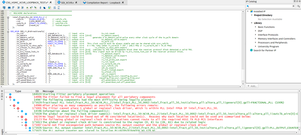
Still trying to instantiate the "SDI II Intel FPGA IP" core. I tried creating another PLL. This time with the "Fractional" option to output the 74.25MHz signal.
I am still getting a Fitter Error.
Info (184020): Starting Fitter periphery placement operations
Error (14996): The Fitter failed to find a legal placement for all periphery components
Info (14987): The following components had the most difficulty being legally placed:
Info (175029): fractional PLL intel_fract_PLL_50:XCVR_PLL_2|intel_fract_PLL_50_0002:intel_fract_pll_50_inst|altera_pll:altera_pll_i|general[0].gpll~FRACTIONAL_PLL (100%)
Error (14986): After placing as many components as possible, the following errors remain:
Error (175001): The Fitter cannot place 1 global or regional clock driver, which is within PLL Intel FPGA IP intel_fract_PLL_50.
Info (14596): Information about the failing component(s):
Info (175028): The global or regional clock driver name(s): intel_fract_PLL_50:XCVR_PLL_2|intel_fract_PLL_50_0002:intel_fract_pll_50_inst|altera_pll:altera_pll_i|outclk_wire[0]~CLKENA0
Error (16234): No legal location could be found out of 46 considered location(s). Reasons why each location could not be used are summarized below:
Error (15123): The following global or regional clock driver locations cannot route to all the required HSSI TX PLD PCS Interfaces
Info (175027): Destination: HSSI TX PLD PCS Interface SDI_XCVR:SDI_ii_Bidirectional1|SDI_XCVR_0002:sdi_xcvr_inst|altera_xcvr_native_av:u_phy|av_xcvr_native:gen_native_inst.av_xcvr_native_insts[0].gen_bonded_group_native.av_xcvr_native_inst|av_pcs:inst_av_pcs|av_pcs_ch:ch[0].inst_av_pcs_ch|av_hssi_tx_pld_pcs_interface_rbc:inst_av_hssi_tx_pld_pcs_interface|wys
Info (175029): 16 locations affected
Info (175029): CLKCTRL_R82
Info (175029): CLKCTRL_R83
Info (175029): CLKCTRL_R84
Info (175029): CLKCTRL_R85
Info (175029): CLKCTRL_R86
Info (175029): CLKCTRL_R87
Info (175029): CLKCTRL_R10
Info (175029): CLKCTRL_R11
Info (175029): CLKCTRL_R12
Info (175029): CLKCTRL_R13
Info (175029): CLKCTRL_R14
Info (175029): CLKCTRL_R15
Info (175029): and 4 more locations not displayed
Info (175013): The global or regional clock driver is constrained to the region (0,
Info (175015): The I/O pad CLOCK_50_B7A is constrained to the location PIN_H12 due to: User Location Constraints (PIN_H12)
Info (14709): The constrained I/O pad is contained within a pin, which drives a fractional PLL, which drives a PLL output counter, which drives this global or regional clock driver
Error (175007): Could not find uncongested path between source PLL output counter and the global or regional clock driver
Info (175026): Source: PLL output counter intel_fract_PLL_50:XCVR_PLL_2|intel_fract_PLL_50_0002:intel_fract_pll_50_inst|altera_pll:altera_pll_i|general[0].gpll~PLL_OUTPUT_COUNTER
Info (175013): The PLL output counter is constrained to the region (0, 17) to (0, 33) due to related logic
Info (175015): The I/O pad CLOCK_50_B7A is constrained to the location PIN_H12 due to: User Location Constraints (PIN_H12)
Info (14709): The constrained I/O pad is contained within a pin, which drives a fractional PLL, which drives this PLL output counter
Info (175021): The PLL output counter was placed in location PLLOUTPUTCOUNTER_X0_Y29_N1
Error (175022): The global or regional clock driver could not be placed in any location to satisfy its connectivity requirements
Info (175029): 30 locations affected
Info (175029): CLKCTRL_G0
Info (175029): CLKCTRL_G1
Info (175029): CLKCTRL_G2
Info (175029): CLKCTRL_G3
Info (175029): CLKCTRL_R64
Info (175029): CLKCTRL_R65
Info (175029): CLKCTRL_R66
Info (175029): CLKCTRL_R67
Info (175029): CLKCTRL_R68
Info (175029): CLKCTRL_R69
Info (175029): CLKCTRL_R40
Info (175029): CLKCTRL_R41
Info (175029): and 18 more locations not displayed
Info (184021): Fitter periphery placement operations ending: elapsed time is 00:00:00
- Mark as New
- Bookmark
- Subscribe
- Mute
- Subscribe to RSS Feed
- Permalink
- Report Inappropriate Content
One idea I have about this error message is that the Clock pin I'm using for the PLL (CLOCK_50_B7A on Bank 7) is on a separate bank from the Tx & Rx pins (which are on bank GXB_L0). If that is the case, then I only have REFCLK_p0 to work with as the input to the PLL since it is on the same bank as the Rx & Tx pins I am trying to connect together. Does that sound about right?
- Mark as New
- Bookmark
- Subscribe
- Mute
- Subscribe to RSS Feed
- Permalink
- Report Inappropriate Content
OK, using the REFCLK_p0 is one step further. I can compile it now when I replace the xcvr_refclk input from the PLL to the REFCLK_p0 pin. I believe on the C5G starter kit board the REFCLK_p0 pin is fixed at 125MHz. The project however still does not work as intended. The signal going into the RX pin is not coming out the TX pin. Here is the newer updated QAR attached.
Here is a picture of the RTL viewer:
I had hooked the "Tx_dataout_valid" signal right back into the "tx_datain_valid" signal but I'm not sure if that is right.
Please help.
- Mark as New
- Bookmark
- Subscribe
- Mute
- Subscribe to RSS Feed
- Permalink
- Report Inappropriate Content
Hi,
Few question for you.
Q1. What are you feeding to TX as an input, there must be some initial value?
Q2. If there is how are you feeding it?
Even though you feed some constant value to the transmit, there is higher probability you will see the bit shift at the receiver. You need to reconstruct the word or design a word aligner in the FPGA fabric.
On top of everything, you should not try in this way of looping back.
Thank you
Kshitij Goel
- Mark as New
- Bookmark
- Subscribe
- Mute
- Subscribe to RSS Feed
- Permalink
- Report Inappropriate Content
I am feeding Rx into Tx, so Tx initial value will be the same as Rx.
I have tried to loop all the Rx wires into the Tx inputs.
Here is where I am feeding the Tx:
.tx_datain ( SDI_Databus20 ), // input wire [19:0] tx_datain.export
.tx_datain_valid ( Tx_dataout_valid ),// input wire generate a tx_datain_valid pulse every other clock cycle of the tx_pclk domain
.tx_dataout_valid ( Tx_dataout_valid ),// output wire tx_dataout_valid.export
.tx_pclk ( FRACT_74_25MHZ ), // input wire tx_pclk.clk
.tx_coreclk_hd ( FRACT_74_25MHZ ), // input wire This clock source must be always stable and can be shared with xcvr_refclk
.rx_coreclk_is_ntsc_paln ( 1'b0 ), // input wire 0 = PAL rate (when rx_coreclk = 297 / 148.5 MHz or rx_coreclk_hd = 74.25 MHz)
.rx_clkout_is_ntsc_paln ( ), // output wire rx_clkout_is_ntsc_paln.export
.rx_trs_in ( ), // input wire [0:0] indicate to the PHY management block that the receiver protocol block detected a valid TRS.
.rx_trs_loose_lock_in ( ), // input wire [0:0] This signal must be driven by rx_trs_loose_lock_out of the receiver protocol block.
.rx_dataout ( SDI_Databus20 ), // output wire [19:0] rx_dataout.export
.rx_dataout_valid ( ), // output wire rx_dataout_valid.export
.rx_clkout ( ), // output wire rx_clkout.clk
.rx_rst_proto_out ( ), // output wire rx_rst_proto_out.export
.rx_rst ( ~reset_n ), // input wire rx_rst.reset
.rx_coreclk_hd ( FRACT_74_25MHZ ), // input wire rx_coreclk_hd.clk
.xcvr_refclk ( REFCLK_p0 ), // input wire << Must be on the Same BANK as the sdi_tx & sdi_rx FPGA pins.
.sdi_tx ( HSMC_GXB_TX_p ), // output wire sdi_tx.export
.tx_pll_locked ( ), // output wire tx_pll_locked.export
.tx_clkout ( ), // output wire tx_clkout.clk
.sdi_rx ( HSMC_GXB_RX_p ), // input wire sdi_rx.export
- Mark as New
- Bookmark
- Subscribe
- Mute
- Subscribe to RSS Feed
- Permalink
- Report Inappropriate Content
"On top of everything, you should not try in this way of looping back." -K**bleep**ij Goel
My question from the beginning, has been: What is the best way to connect the HSMC_GXB_RX pin to the HSMC_GXB_TX pin together inside the FPGA?
Please suggest what is the best way to try this way of looping back.
- Subscribe to RSS Feed
- Mark Topic as New
- Mark Topic as Read
- Float this Topic for Current User
- Bookmark
- Subscribe
- Printer Friendly Page
