- Mark as New
- Bookmark
- Subscribe
- Mute
- Subscribe to RSS Feed
- Permalink
- Report Inappropriate Content
hey to you all,
im trying to interface to ddr3 component with the ddr3 uniphy controller ip .
im using cyclone v soc development kit with quartus version 14.1 .
i succeded to run the example design that intel provides and it runs successfully.
the interface between the example driver to the ddr3 uniphy controller ip is avalon mm interface.
what im trying to understand is the local address mapping in the avalon mm vs the address on the memory itself.
avalon local address bus : [29:0]
mem_a:[14:0]
could you explain the address mapping with read/write example?
thanks,
BR,
Ram.
- Mark as New
- Bookmark
- Subscribe
- Mute
- Subscribe to RSS Feed
- Permalink
- Report Inappropriate Content
hello again,
ok i think i understands the addressing now.
the address[29:0] uses only [29:4].(26 bits out of 30). and the 4 bits left are just padding.
correct me if im wrong.
thanks,
Ram.
Link Copied
- Mark as New
- Bookmark
- Subscribe
- Mute
- Subscribe to RSS Feed
- Permalink
- Report Inappropriate Content
Hi Ram,
Thank you for submitting your question in Intel Community.
I'm Adzim will assist you in this thread.
The avalon local address is a parameter that store the location of the bank that to be accessed during the read and write memory transaction.
It's combination of chip select bits + row bits + bank bits + column - N where N is 1 for full-rate controller and 2 for half-rate controller.
The order of address mapping is based on the "Local-to-Memory Address Mapping" setting in the IP.
The memory address is determined the operation of the memory. This can be referred to memory datasheet in the truth table.
For read and write operation, there is timing diagram that illustrated the read and write operation in the EMIF handbook volume 3 starting on page 440.
Link: https://www.intel.com/programmable/technical-pdfs/683841.pdf#page=440
Regards,
Adzim
- Mark as New
- Bookmark
- Subscribe
- Mute
- Subscribe to RSS Feed
- Permalink
- Report Inappropriate Content
hey Adzim,
thank you for the fast answer.
things are more clearly now.
still there is somthing that i dont understand.
we are using the Micron device https://media.digikey.com/pdf/Data%20Sheets/Micron%20Technology%20Inc%20PDFs/MT41K256M16_MT41K1G4_MT41K512M8_DS.pdf
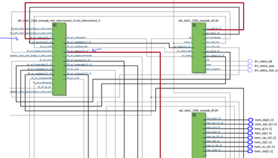
according to the equation i can see that the address is 26 bits wide.
still there is a different between the address before the avalon interconnect and after the avalon interconnect as showing in the picture below.
why there is such a difference?
BR,
Ram.
- Mark as New
- Bookmark
- Subscribe
- Mute
- Subscribe to RSS Feed
- Permalink
- Report Inappropriate Content
hello again,
ok i think i understands the addressing now.
the address[29:0] uses only [29:4].(26 bits out of 30). and the 4 bits left are just padding.
correct me if im wrong.
thanks,
Ram.
- Mark as New
- Bookmark
- Subscribe
- Mute
- Subscribe to RSS Feed
- Permalink
- Report Inappropriate Content
Hi Ram,
Yes you are correct.
Is there any further question on this thread?
Regards,
Adzim
- Mark as New
- Bookmark
- Subscribe
- Mute
- Subscribe to RSS Feed
- Permalink
- Report Inappropriate Content
yes thank you.
- Mark as New
- Bookmark
- Subscribe
- Mute
- Subscribe to RSS Feed
- Permalink
- Report Inappropriate Content
I’m glad that your question has been addressed, I now transition this thread to community support. If you have a new question, feel free to open a new thread to get the support from Intel experts. Otherwise, the community users will continue to help you on this thread. Thank you.
- Subscribe to RSS Feed
- Mark Topic as New
- Mark Topic as Read
- Float this Topic for Current User
- Bookmark
- Subscribe
- Printer Friendly Page
