- Mark as New
- Bookmark
- Subscribe
- Mute
- Subscribe to RSS Feed
- Permalink
- Report Inappropriate Content
Hi,
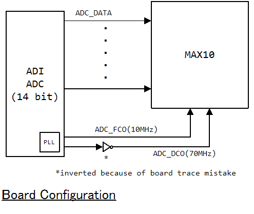
I have a project in which MAX10 has an external ADC that has LVDS connections-- data, ADC_DCO, ADC_FCO.
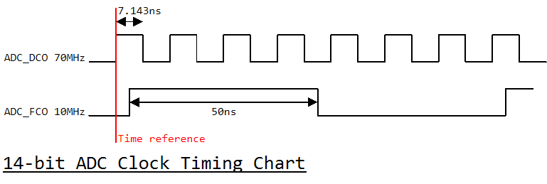
I wrote a constraint for external clocks like the next picture, but Timing Analyzer doesn't recognize the delayed rising edge of ADC_FCO to ADC_DCO.
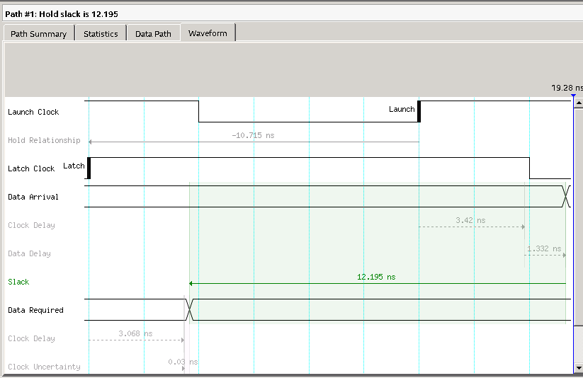
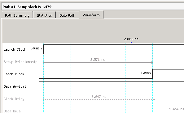
Both the launch edge and the latch edge rise at the same time. Then Timing Analyzer reports a lack of setup time. Why Timing Analyzer doesn't recognize my phase-shift clock constraint?
My constraint:
create_clock -name ADC_DCO -period 14.286 -waveform {0 7.143} [get_ports {ADC_DCO ADC_DCO(n)}]
create_clock -name ADC_FCO -period 100 -waveform {3.571 53.571} [get_ports {ADC_FCO ADC_FCO(n)}]
Timing Analyzer read the constraint above.
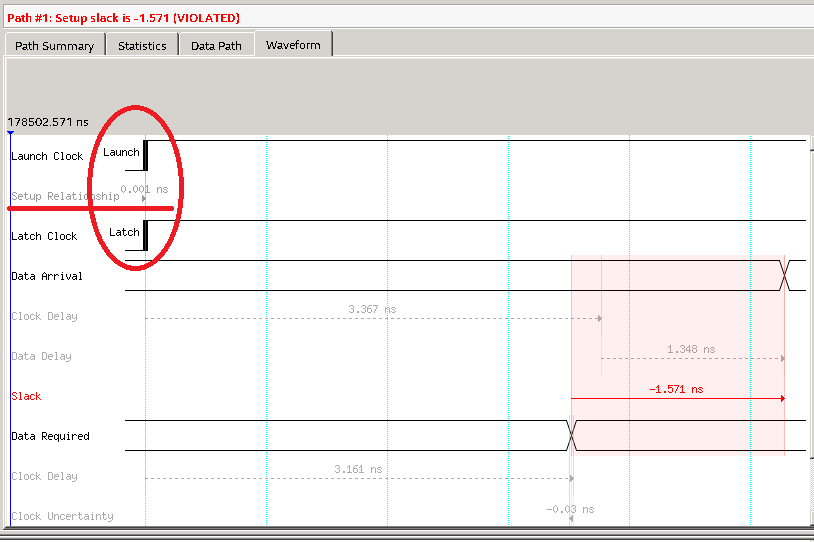
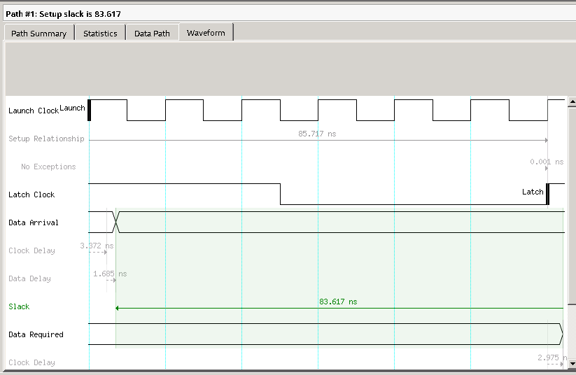
Timing Analyzer reported a setup error.
In the waveform view, the launch edge (ADC_DCO) and the latch edge (ADC_FCO) rise at the sate time. The Setup Relationship is almost 0. Naturally, the setup time is not satisfied. Why the latch edge doesn't delay to the launch edge?
Thanks in advance.
HKana17
My environment
Quartus Prime Lite Edition: 18.1.0 Build 625 09/12/2018 SJ Lite Edition
Windows7 professional sp1
Target device: MAX 10 (10M08)
- Mark as New
- Bookmark
- Subscribe
- Mute
- Subscribe to RSS Feed
- Permalink
- Report Inappropriate Content
After looking at the Board Configuration, I believe this is Source-Synchronous Interface.
You may refer to the AN 433: Constraining and Analyzing Source-Synchronous Interfaces, section "Input Clock Constraints" on how to constraint the clock.
With the current clock constraints you have, they are not synchronous with each other. Therefore, meeting either the phase-shift or frequency requirement cannot fulfill both requirements simultaneously.
One approach I can suggest is to write a clock constraint in such a way that Quartus treats this as a PLL, ensuring that both clocks are synchronous with each other.
Regards,
Richard Tan
Link Copied
- Mark as New
- Bookmark
- Subscribe
- Mute
- Subscribe to RSS Feed
- Permalink
- Report Inappropriate Content
With those fractional frequencies, I don't think the two clocks are exactly synchronous to each other, so they are going to line up at some point, which the timing analyzer is pointing out.
3.571 x 4 = 14.284 < 14.286
- Mark as New
- Bookmark
- Subscribe
- Mute
- Subscribe to RSS Feed
- Permalink
- Report Inappropriate Content
How is the hold slack with the same timing path? If the hold has enough window, perhaps you can use set_min_delay sdc constraint to the path.
Could you please share your design by archiving the project (Project > Archive Project) so that I can investigate it further?
Regards,
Richard Tan
- Mark as New
- Bookmark
- Subscribe
- Mute
- Subscribe to RSS Feed
- Permalink
- Report Inappropriate Content
Guys, thank you for your reply.
And nice to see you again.
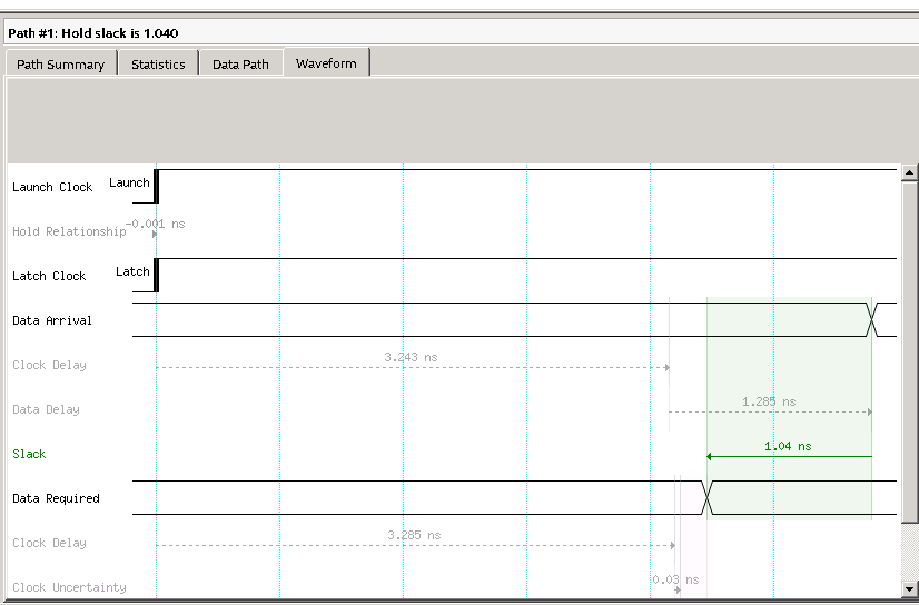
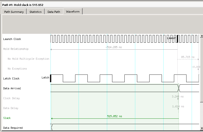
Here is the hold time slack on the same path. It is 1.040 ns.
I can't disclose the whole project file because I am developing this with my customer.
ADC_FCO clock is the timing frame signal of the ADC. So ADC_DCO clock and ADC_FCO clock are synchronized. How can I tell Timing Analyzer these kinds of clocks?
Best regards,
HKana17
- Mark as New
- Bookmark
- Subscribe
- Mute
- Subscribe to RSS Feed
- Permalink
- Report Inappropriate Content
The frequencies have to be exact multiples of each other. Even in that hold timing analysis that is passing, the clock edges are incorrect compared to your diagram up top, further proving what I was saying.
- Mark as New
- Bookmark
- Subscribe
- Mute
- Subscribe to RSS Feed
- Permalink
- Report Inappropriate Content
Thank you for your reply.
Do you mean using the "-divide_by" or "-multiply_by" option for external clocks? I think they are for generated clocks or internal PLL clocks...
How can I write a constraint for external clocks synchronized with each other in my case? I saw "Intel Quartus Prime Timing Analyzer Cookbook" before making a question.
Best regards,
HKana17
- Mark as New
- Bookmark
- Subscribe
- Mute
- Subscribe to RSS Feed
- Permalink
- Report Inappropriate Content
Like I said, you're using decimal frequencies/phase shifts that are not exactly multiples of each other in your constraints. Why can't they be:
create_clock -name ADC_DCO -period 14.286 -waveform {0 7.142} [get_ports {ADC_DCO ADC_DCO(n)}]
create_clock -name ADC_FCO -period 100 -waveform {3.571 53.571} [get_ports {ADC_FCO ADC_FCO(n)}]
Better yet, input one clock and use a PLL to generate the 2 synchronous clocks if you can.
These are very odd frequencies and phase shifts to rely on just what is arriving at the device.
- Mark as New
- Bookmark
- Subscribe
- Mute
- Subscribe to RSS Feed
- Permalink
- Report Inappropriate Content
Thank you for your reply.
Do you mean to rewrite 7.143 to 7.142? The waveform option affects its duty cycle and phase. The frequency is defined by the period option. The ratio 100ns to 14.286ns is almost 7-- 6.99986. Am I wrong? Here, I supposed that the length of traces from the ADC to MAX10 is the same.
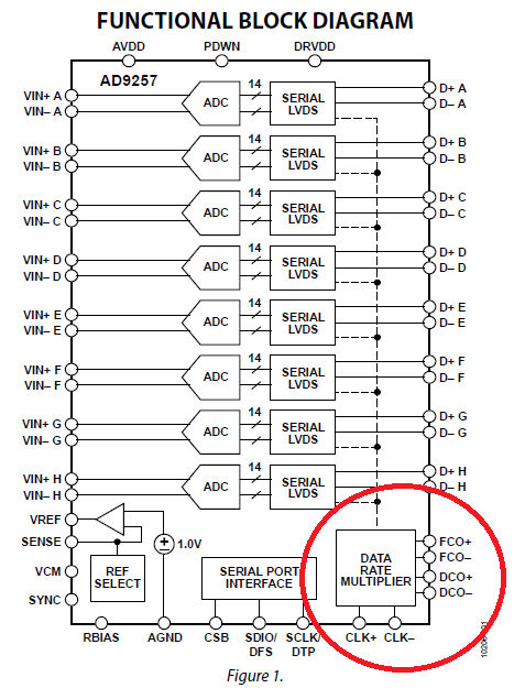
In my case, the PLL exists in the external ADC. Here is the block diagram of the ADC.
The PLL generates the data clock (ADC_DCO) multiplied by 7 times the input clock. The frequency of the frame clock (ADC_FCO) is the same as the input clock and phase-shifted precisely to ADC_DCO. Here is the timing chart. (But in my board, because of the miss of the board trace DCO polarization is inverted.)
Again how can I write a constraint for this configuration?
Regards,
HKana17
- Mark as New
- Bookmark
- Subscribe
- Mute
- Subscribe to RSS Feed
- Permalink
- Report Inappropriate Content
You can try to add set_multicycle_path constraint for fast-to-slow clock.
multicycle -setup with a value of N, and a multicycle -hold with a value of N-1
set_multicycle_path N -setup -from launch_clk(fast) -to latch_clock(slow) -start
set_multicycle_path N-1 -hold -from launch_clk(fast) -to latch_clock(slow)
Regards,
Richard Tan
- Mark as New
- Bookmark
- Subscribe
- Mute
- Subscribe to RSS Feed
- Permalink
- Report Inappropriate Content
Thank you for your reply. I'm glad you didn't forget me.
Now, I added the multi_cycle_path constraint you taught me.
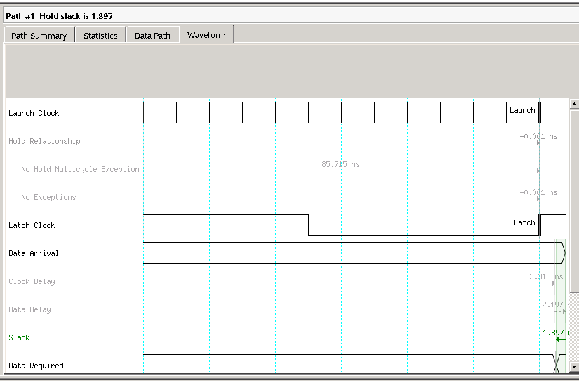
It's true that the timing between the launch and the latch clocks changes.
Setup
Setup Waveform
Hold
Hold Waveform
But isn't it different from what you expected?
Regards,
HKana17
- Mark as New
- Bookmark
- Subscribe
- Mute
- Subscribe to RSS Feed
- Permalink
- Report Inappropriate Content
My bad, I noticed the hold is -end instead of -start. FYI we use -end for both setup and hold, for slow-to-fast clock.
Use these constraints instead.
set_multicycle_path N -setup -from launch_clk(fast) -to latch_clock(slow) -start

set_multicycle_path N-1 -hold -from launch_clk(fast) -to latch_clock(slow) -start
Regards,
Richard Tan
- Mark as New
- Bookmark
- Subscribe
- Mute
- Subscribe to RSS Feed
- Permalink
- Report Inappropriate Content
Thank you for your suggestion. I added -start option. The hold-time timing chart varied. But the rising edge of 2 waveforms is still at the same time. I think it is necessary to shift the edge time between 2 signals rather than the multiplier factor.
And I don't know the set_multicycle_path option well. Do you know a good text of a sdc file grammar?
Regards,
HKana17
- Mark as New
- Bookmark
- Subscribe
- Mute
- Subscribe to RSS Feed
- Permalink
- Report Inappropriate Content
I think I might have misunderstood your question regarding how to phase shift the clock. Initially, I was focused on closing the design timing.
The recommended solution is to first reconfigurable your IOPLL, then use dynamic phase shift to achieve the phase shift you want.
Please refer to this UG. Section 2.3.11.3. Programmable Phase Shift
https://cdrdv2-public.intel.com/666937/ug_m10_clkpll-683047-666937.pdf
Regards,
Richard Tan
- Mark as New
- Bookmark
- Subscribe
- Mute
- Subscribe to RSS Feed
- Permalink
- Report Inappropriate Content
Dropping a note to ask if my last reply was helpful to you?
Do you need any further assistance from my side?
Regards,
Richard Tan
- Mark as New
- Bookmark
- Subscribe
- Mute
- Subscribe to RSS Feed
- Permalink
- Report Inappropriate Content
Thank you for your comments. But my question isn't solved. The question is how to make a constraint for external clocks (ADC_DCO & ADC_FCO) provided by an external ADC. Their phase is precisely as described in the ADC timing chart of the datasheet (I gave the timing chart before.).
I will add some supplement explanations to the first post later.
Regards,
HKana17
- Mark as New
- Bookmark
- Subscribe
- Mute
- Subscribe to RSS Feed
- Permalink
- Report Inappropriate Content
Since these clocks are external clock, use create_clock (without the -target), to add a virtual clock for the I/O interface.
example: create_clock -period 5.0 -name dac_clk_ext
Note that I did not apply these clocks to anything in the FPGA, which is what makes them virtual clocks; they exist outside of the FPGA.
Manually phase-shifting a clock, usually done with a PLL. Try to use the create_generated_clock so that the generated clocks are related, so crossings between them are not asynchronous.
# Create a virtual clock, and two generated clocks that derive from it.
# This makes the generated clocks related, so crossings between them are not asynchronous.
create_clock -period 10 -name virtual_base
create_generated_clock -master_clock virtual_base -divide_by 2 [get_ports clka]
create_generated_clock -master_clock virtual_base -divide_by 4 [get_ports clkb]
As mentioned by Sstrell in the previous post, the frequencies have to be exact multiples of each other.
Regards,
Richard Tan
- Mark as New
- Bookmark
- Subscribe
- Mute
- Subscribe to RSS Feed
- Permalink
- Report Inappropriate Content
Thank you for your comments. But you say difficult things for me. I wonder whether such complicated constraints are necessary to implement a deserializer of ADC output.
Today I modified the ADC_FCO period in the sdc file for another need. I changed the period parameter from 100 to 28.572. It is just two times to the period of the ADC_DCO clock (14.286), with a pico-second unit.
create_clock -name ADC_DCO -period 14.286 -waveform {0 7.143} [get_ports {ADC_DCO ADC_DCO(n)}]
create_clock -name ADC_FCO -period 28.572 -waveform {3.571 17.857} [get_ports {ADC_FCO ADC_FCO(n)}]
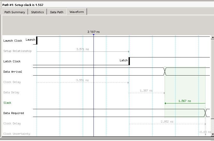
Then what I expected for a long time occurred. The edge of the ADC_FCO is located 3.571 ns away from the ADC_DCO edge. Here it is!
Is it a point to write period time multiplied by an integer instead of actual period one, with a pico-second unit?
Setup
Hold
Regards,
HKana17
- Mark as New
- Bookmark
- Subscribe
- Mute
- Subscribe to RSS Feed
- Permalink
- Report Inappropriate Content
Hi.
I modified the period time to 100.002 (ps) in my ADC_FCO constraint like below.
create_clock -name ADC_FCO -period 100.002 -waveform {3.571 53.571} [get_ports {ADC_FCO ADC_FCO(n)}]
The clock frequency of ADC_FCO is just 10.000MHz. So the real period is 100.000ns. 100.002 is the number multiplied by 7 of the ADC_DCO period (14.286).
Is this the trick here? Where can I see this in Intel's (Altera's) documents?
Regards,
HKana17
- Mark as New
- Bookmark
- Subscribe
- Mute
- Subscribe to RSS Feed
- Permalink
- Report Inappropriate Content
Excuse me. I forgot to write an important thing.
I succeeded it with the 100.002's clock constraint.
- Mark as New
- Bookmark
- Subscribe
- Mute
- Subscribe to RSS Feed
- Permalink
- Report Inappropriate Content
In your case, I believe it is recommended to multiply by an integer instead, as it will meet your requirement of ensuring the clocks are phase-shifted.
If not using an exact multiplier, the phase shift difference will either get closer or further away, eventually not meeting the desired phase shift.
Sorry for the confusion, may I know is the clock constrained is inside the FPGA or outside the FPGA?
Regards,
Richard Tan
- Mark as New
- Bookmark
- Subscribe
- Mute
- Subscribe to RSS Feed
- Permalink
- Report Inappropriate Content
Thank you for your comments.
Here is the configuration drawing.
I mean constraints for circuits on MAX10 inside. Suppose that traces from the ADC to MAX10 are the same length.
- Subscribe to RSS Feed
- Mark Topic as New
- Mark Topic as Read
- Float this Topic for Current User
- Bookmark
- Subscribe
- Printer Friendly Page
