- Mark as New
- Bookmark
- Subscribe
- Mute
- Subscribe to RSS Feed
- Permalink
- Report Inappropriate Content
Note: This article is an English translation of this Japanese article. Please refer to the original article for updates.
Introduction
This article targets those who are new to FPGA, covering the overview, installation, hardware construction, and execution of Hello World for the Nios® V/m embedded processor. Those who already have experience with FPGA may skim through certain parts like the installation.
The Operating Systems used for operational verification are as follows:
- Windows 11 Enterprise Version: 22H2, Build: 22621.2715
- Ubuntu 22.04.3 LTS (Jammy Jellyfish), Kernel version: 6.2.0-36-generic
The work will primarily be conducted on Linux, and explanations will include actual logs. However, when commands differ significantly on Windows, they will be explained as necessary.
Below are reference materials for the Nios® V/m embedded processor:
- Nios® V Embedded Processor Design Handbook
- Nios® V Processor Reference Manual
- NiosV tool setup for Eclipse CDT and OpenOCD
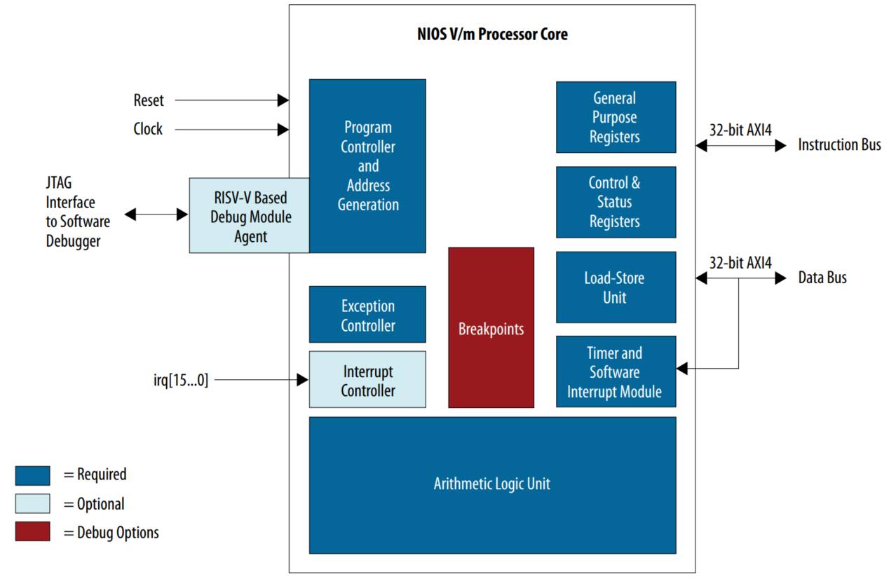
1. Overview of the Nios® V/m Embedded Processor
1.1 Instruction Set
The Nios® V/m embedded processor supports the RV32IA instruction set. RV32I denotes a 32-bit integer instruction set, and the symbols following it indicate extensions. The main extensions are listed below.
Extension Description
| M | Integer Multiplication and Division |
| A | Atomic Instructions |
| F | Single-Precision Floating-Point |
| D | Double-Precision Floating-Point |
| Q | Quad-Precision Floating-Point |
| C | Compressed Instructions |
Therefore, R32IA supports 32-bit integer instructions and atomic instructions. The processor has 32 32-bit wide integer registers, implemented using block memories like M20K. As indicated by the extension symbols, floating-point registers (f0-f31, fcsr) are not implemented. For more details, please refer to RISC-V Unprivileged Spec v.20191213.
1.2 Configuration
The basic configuration is shown below.
Item Details
| General Purpose Register file | 32-bit width x 32 integer general-purpose register file |
| Arithmetic Logic Unit (ALU) | Performs arithmetic, comparison, logical, and shift operations. Also used for generating addresses for loads and stores |
| Control and Status Registers (CSR) | Control registers |
| Exception Controller | Exception processing controller |
| Interrupt Controller | Interrupt controller, level-triggered |
| Instruction Bus | Instruction bus |
| Data Bus | Data bus |
| RISC-V based Debug Module | Debug module |
Here are the main differences from Nios® II:
Item Nios® V/m Embedded Processor Nios® II
| Bus | Arm* ABMA* AXI | Avalon-MM |
| Number of Interrupt Terminals | 16 | 32 |
| Debug | Open OCD (On-Chip Debugger) compliant | Proprietary specification |
1.3 Instruction, Data Bus
While Nios® II used the Avalon-MM bus, the Nios® V/m Processor has switched to Arm* ABMA* AXI. This change allows for exceptions to be triggered in the Nios® V/m Processor when the response from AXI is not OK. The types of AXI responses are as follows:
RESP[1:0] Response Description
| 2'b00 | OKAY | Normal access OK |
| 2'b01 | EXOKAY | Exclusive access OK |
| 2'b10 | SLVERR | Slave returned an error |
| 2'b11 | DECERR | No slave at the specified address |
For more details, please refer to Read and Write Response Structure.
1.4 Pipeline
The Nios® V/m embedded processor is a 5-stage pipeline CPU. An overview of each stage is provided below.
Stage Denotation Function
| Instruction Fetch | F | • PC+4 calculation<br>• Next instruction fetch<br>• Pre-decode for register file read |
| Instruction Decode | D | • Decode the instruction<br>• Register file read data available<br>• Hazard resolution and data forwarding |
| Instruction Execute | E | • ALU operations<br>• Memory address calculation<br>• Branch resolution<br>• CSR read/write |
| Memory | M | • Memory and multicycle operations<br>• Register file write<br>• Branch redirection |
| Write Back | W | • Facilitates data dependency resolution by providing General Purpose Register value. |
1.5 Exceptions
The exceptions currently defined are as follows:
Exception Description
| Instruction Address Misaligned | Exception is issued when the Program Counter (PC) is not aligned on a 32-bit boundary during the instruction fetch stage (i.e., the lower 2 bits of the PC are not zero). |
| Instruction Access Fault | Exception is issued if the AXI response during instruction read is not OKAY. |
| Illegal Instruction | Exception is issued if an unimplemented or undefined instruction is detected during instruction decode, or if an unimplemented or undefined CSR access is detected during the execute stage. |
| Breakpoint | Exception is issued at the decode stage when a break instruction is executed. |
| Load Address Misaligned<br>Store/AMO Address Misaligned | Exception is issued during the memory access stage if the load/store instruction's address is not aligned with the access size. |
| Load Access Fault<br>Store/AMO Access Fault | Exception is issued if the AXI bus returns a response other than OKAY during memory access. |
| Environment Call from U-mode | Exception is issued when ECALL instruction is executed in U-mode. |
| Environment Call from S-mode | Exception is issued when ECALL instruction is executed in S-mode. |
| Environment Call from M-mode | Exception is issued when ECALL instruction is executed in M-mode. |
| Instruction Page Fault<br>Load Page Fault<br>Store/AMO Page Fault | Exception is issued when accessing a virtual address that does not correspond to a physical address, or when access rights are insufficient. |
1.6 CSR Registers
The registers mapped in the CSR area are shown below. For more details on the registers, please refer to RISC-V Privileged Spec v.20190608.
Register Name Description
| mvendorid | Machine Vendor ID Register |
| marchid | Machine Architecture ID Register |
| mimpid | Machine Implementation ID Register |
| mhartid | Hart ID Register |
| mstatus | Machine Status Register |
| mtvec | Machine Trap-Vector Base-Address Register |
| mip | Machine Interrupt-pending Register |
| mie | Machine Interrupt-enable Register |
| mcounteren | Machine Counter-enable Register |
| mepc | Machine Exception Program Counter |
| mcause | Machine Cause Register |
The registers mapped in the memory-mapped area are shown below.
Register Name Description Offset
| mtimecmp | Machine Time Register | 0x00 |
| mtime | Machine Time Register | 0x08 |
1.7 Supported Devices
The FPGA devices currently supported are as follows:
Intel® Quartus® Prime Edition Device Family
| Pro | Intel® Cyclone® 10 device |
| Pro | Intel® Arria® 10 device |
| Pro | Intel® Stratix® 10 device |
| Pro | Intel Agilex® 7 device |
| Standard | Intel® MAX® 10 |
| Standard | Intel® Cyclone® IV E |
| Standard | Intel® Cyclone® IV GX |
| Standard | Intel® Cyclone® V |
| Standard | Intel® Cyclone® 10 LP |
| Standard | Intel® Arria® 10 |
| Standard | Intel® Arria® II GX |
| Standard | Intel® Arria® II GZ |
| Standard | Intel® Arria® V |
| Standard | Intel® Arria® V GZ |
| Standard | Intel® Stratix® IV |
| Standard | Intel® Stratix® V |
2. Obtaining a License
To use the Nios® V/m embedded processor, you need to acquire a free license. This section explains the procedure for obtaining a license. Additionally, we will also obtain a license for Questa*-Intel® FPGA Edition Software, used as a simulator.
2.1 Sign In
Click on the Self Service Licensing Center. A Sign In screen like the one below will appear, so please sign in with your Intel account.

If you do not have an Intel account, please create one.
2.2 Obtaining a Nios® V/m Embedded Processor License
After signing in, the following screen will appear.

Select Intel® FPGA IP IP-NIOSVM, enter "1" in "# of Seats", and click "Get License" at the bottom right.
2.3 Registering a New Computer
The following screen will appear.

If you are obtaining a license for the first time, select "Create a New Computer". If you have already registered, select "Assign an Existing Computer" and click the "Generate" button at the bottom right. This time, we will register a new computer, creating an ID using the Ethernet MAC ID.
2.4 Entering New Computer Information
The following screen will appear, where you set up the computer you are using.

Enter the necessary items below and click "Generate License".
Item Description
| Computer Name | Enter any name |
| License Type | Select FIXED |
| Computer Name | Select NIC ID |
| Primary Computer ID | Enter the PC's Ethernet MAC ID |
2.5 Checking the Nios® V/m Embedded Processor License File
Once generated, the following screen will appear, and the license file will be sent to the registered email address, so please check the file.

2.6 Obtaining a Questa*-Intel® FPGA Edition Software License
Follow the same procedure to obtain a license for Questa*-Intel® FPGA Edition Software. If you already have a license, proceed to the next chapter. As before, click on Self Service Licensing Center.

Select Questa*-Intel® FPGA Starter software Edition SW-QUESTA, enter "1" in "# of Seats", and click "Get License" at the bottom right.
2.7 Adding to an Existing Computer
If the following screen appears, specify the PC you registered earlier by selecting "Assign an Existing Computer", enter the MAC ID, and press the "Generate" button at the bottom right.

2.8 Checking the Questa*-Intel®
FPGA Edition Software License File
Once generated, the following screen will appear, and the license file will be sent to the registered email address.

With this, the process of obtaining the license is complete.
3. Installation
This chapter explains how to download and install Intel® Quartus® Prime Software, and how to set up environment variables.
3.1 Installing Intel® Quartus® Prime Pro Edition 23.3
3.1.1 Download
First, click on the FPGA Software Download Center and go to the page below. Follow the instructions for your OS to click on the corresponding version of Intel® Quartus® Prime Software. This explanation will cover installation on Linux.

Clicking will bring up the following page. Verify that the version is 23.3, then scroll down.

Download the Intel® Quartus® Prime Pro Edition Installer (RUN) from the page below. For Windows, download the Intel® Quartus® Prime Pro Edition Installer (EXE).

Once downloaded, enter the following commands in the download directory to launch the installer:
$ chmod +x *.run
$ ./qinst-linux-23.3-104.run
For Windows, double-click the downloaded qint-windows-23.3-104.exe.
When the installer launches, select:
- Intel® Quartus® Prime Pro Edition Part 1 (includes Nios II EDS)
- Intel® Quartus® Prime Pro Edition Part 2
- Questa*-Intel® FPGA and Starter Editions
- Intel® Arria® 10 device support
- Ashling RiscFree IDE for Intel® FPGAs Check "Agree to Intel License Agreement" and click Download. If you wish to change the download or installation location, do so on this screen.

For Windows, ensure the following are checked under After-install actions:
- Launch USB Blaster driver installation
- Launch USB blaster II driver installation
- Install JTAG Server as a Windows service

During download & installation on Windows, the Device Driver Installation Wizard will open for Intel® FPGA Download Cable II (formerly USB Blaster II) and Intel® FPGA Download Cable (formerly USB Blaster), which are necessary for FPGA configuration and debugging the Nios® V/m embedded processor. Please install them. For Linux, follow "1.6. Installing the Intel FPGA Download Cable II Driver on Linux Systems" in the Intel® FPGA Download Cable II User Guide.
Install the Intel® FPGA Download Cable (formerly USB Blaster) driver. Click Next.

Click Finish.

Install the Intel® FPGA Download Cable II (formerly USB Blaster II) driver. Click Next.

Click Finish.

This is the screen after completing the Quartus installation.

With this, the installation of Intel® Quartus® Prime Pro Edition is complete.
3.2 Setting up Environment Variables
3.2.1 Linux
Execute the following to set paths to tools and specify the license file.
#!/bin/bash
export QUARTUS_ROOTDIR="$HOME/intelFPGA_pro/23.3/quartus"
export QSYS_ROOTDIR="$QUARTUS_ROOTDIR/../qsys/bin"
export SOPC_KIT_NIOS2="${QUARTUS_ROOTDIR}/../nios2eds"

# Tools
QUARTUS="$QUARTUS_ROOTDIR/bin64"
QSYS="$QSYS_ROOTDIR"
NIOSV="$QUARTUS_ROOTDIR/../niosv/bin"
NIOS2EDS="$QUARTUS_ROOTDIR/../nios2eds/bin"
MAKE="$QUARTUS_ROOTDIR/../riscfree/build_tools/bin"
CMAKE="$QUARTUS_ROOTDIR/../riscfree/build_tools/cmake/bin"
GCC="$QUARTUS_ROOTDIR/../riscfree/toolchain/riscv32-unknown-elf/bin"

if [ -d "$QUARTUS_ROOTDIR/../questa_fe" ]; then
    QSIM="$QUARTUS_ROOTDIR/../questa_fe/bin"
elif [ -d "$QUARTUS_ROOTDIR/../questa_fse" ]; then
    QSIM="$QUARTUS_ROOTDIR/../questa_fse/bin"
else
    echo "Questa not found"
fi

export PATH="$QUARTUS:$QSYS:$NIOSV:$NIOS2EDS:$MAKE:$CMAKE:$GCC:$QSIM:$PATH"

# License files
export LM_LICENSE_FILE="$HOME/license/1-V4ICFB_License.dat"
export MGLS_LICENSE_FILE="$HOME/license/1-V4ICFB_License.dat"
Regarding the license, $HOME/license/1-V4ICFB_License.dat is specified. If you have multiple license files, separate them with ":" in the following two lines:
export LM_LICENSE_FILE="$HOME/license/1-V4ICFB_License.dat"
export MGLS_LICENSE_FILE="$HOME/license/1-V4ICFB_License.dat"
For example:
# Example
export LM_LICENSE_FILE="$HOME/license/1-V4ICFB_License.dat:$HOME/license/XXX_License.dat"
export MGLS_LICENSE_FILE="$HOME/license/1-V4ICFB_License.dat:$HOME/license/XXX_License.dat"
3.2.2 Windows
For Windows, use the Nios V Command Shell, so setting the tool paths is not necessary. Only specify the license. Press the Windows key on your keyboard and type "env".

Then select "Edit the system environment variables".
The following dialog opens, click on "Environment Variables".

In the User Environment Variables settings, as shown in the red frame, specify LM_LICENSE_FILE and MGLS_LICENSE_FILE to the license file. If there are multiple files, separate them with ";".

After restarting, the setup is complete.
4. Hardware Construction
4.1 Design Sample & Preparation
Here, we construct a design using the Nios® V/m embedded processor. Please download the Intel® Arria® 10 FPGA - Nios® V/m Processor based Hello World version 23.3 from the FPGA Design Store. The file name is top.par.

Once the download is complete, copy top.par to your work directory.
If your work directory is $HOME/ws, then execute:
cp $HOME/Downloads/top.par $HOME/ws
For Windows, if your work directory is C:\ws, then drag and drop to copy the file.
Next, set up the environment variables in Terminal for Linux or launch Nios V Command Shell (Quartus Prime Pro 23.3) from the Start menu in Windows.
Move to $HOME/ws and execute the following:
quartus top.par &
When Quartus launches, it will ask for the location to expand the Example Design. Specify your preferred work directory and click OK. From now on, we will proceed assuming the Example Design is expanded in $HOME/ws/top_project for Linux and C:/ws/top_project for Windows. All terminal commands should be executed from $HOME/ws/top_project or C:/ws/top_project.

As you can see in $HOME/ws/top_project/hw/top.v, this design uses only one 50MHz clock input, making it easy to port to other FPGAs. For more details, see 4.5 Porting to Other FPGAs. For the reset, we use an IP that controls signals from JTAG called ISSP (In-System Source & Probe) and perform the reset with toggle_issp.tcl. For more details, see 5.1.6 CPU Reset by ISSP (In-System Source & Probe).
File Description
| readme.txt | README file |
| hw/top.qpf | Quartus Project file |
| hw/top.qsf | Quartus Settings file |
| hw/top.sdc | Synopsys Design Constraints file |
| hw/top.v | Design TOP RTL file |
| scripts/create_qsys.tcl | Platform Designer creation script |
| scripts/toggle_issp.tcl | Reset execution script |
| sw/app_hal/hello.c | Main file for HAL Hello World |
| sw/app_ucosii/hello_ucosii.c | Main file for uC/OS-II Hello World |
| sw/app_freertos/hello_freertos.c | Main file for FreeRTOS™ Hello World |
As a premise, the Example Design just downloaded and expanded is in a ready-to-test state, meaning all files and binaries required for running the Nios® V/m embedded processor are already included. The FPGA configuration file is at $HOME/ws/top_project/ready_to_test/top.sof, and the ELF files for the Nios® V/m embedded processor application are at $HOME/ws/top_project/ready_to_test/app_hal.elf, $HOME/ws/top_project/ready_to_test/app_ucosii.elf, $HOME/ws/top_project/ready_to_test/app_freertos.elf. Use these for testing on actual hardware. The following will explain the steps for compiling the hardware design and building the application for the Nios® V/m embedded processor.
4.2 Checking the Platform Designer Design
Let's check the Platform Designer design in the GUI. There are two ways to launch Platform Designer: one is to launch it from the Intel® Quartus® Prime software, and the other is to launch it via command from the Terminal.
4.2.1 Launching Platform Designer from Intel® Quartus® Prime Software
- Execute the following in the Terminal to launch Quartus:
quartus &
For Windows, you can also launch Quartus from the Start menu by selecting Quartus Prime Pro Edition 23.3.0.104 -> Quartus (Quartus Prime Pro 23.3).

From the File menu, select "Open Project..." and specify $HOME/ws/top_project/hw/top.qpf, then click "Open".
From the Tools menu, select "Platform Designer".
In the "Open System" dialog that appears, click the red frame and specify the $HOME/ws/top_project/hw/sys.qsys file.

- Click Open.
4.2.2 Launching Platform Designer from Terminal
Move to $HOME/ws/top_project and enter the following command:
qsys-edit --quartus-project=hw/top.qpf hw/sys.qsys
4.2.3 Platform Designer Design
Here, we'll check the design configuration and settings for each IP. The following is the overall design configuration:

4.2.3.1 Clock
This is the configuration screen for the clock input IP. If the input clock differs, change this value. If you change it, also modify the clock period in top.sdc (period is specified in ns).

For IP details, please refer to 7.1.1. Clock Bridge Intel® FPGA IP.
4.2.3.2 Reset
This is the configuration screen for the reset input IP.

For IP details, refer to 6.6.3. Reset Bridge.
4.2.3.3 Nios® V/m Embedded Processor
This is the configuration screen for the Nios® V/m embedded processor IP.

For details on each parameter, refer to the following:
- 2.1.1.2.1. Debug Tab
- 2.1.1.2.2. Use Reset Request Tab
- 2.1.1.2.3. Vectors Tab
- 2.1.1.2.4. CPU Architecture
- 2.1.1.2.5. ECC Tab
4.2.3.4 Internal RAM
This is the configuration screen for the internal RAM IP.

For details on each parameter, refer to the following:
- 25.2.1. Memory Type
- 25.2.2. Size
- 25.2.3. Read Latency
- 25.2.4. ROM/RAM Memory Protection
- 25.2.5. ECC Parameter
4.2.3.5 JTAG UART
This is the configuration screen for the JTAG UART IP.

For details on each parameter, refer to the following:
Once you have confirmed the settings, please close Platform Designer.
4.3 Compiling the Design
Next, execute the following command in the Terminal to start compiling the design:
quartus_sh --flow compile hw/top
Output:
Info: *******************************************************************
Info: Running Quartus Prime Shell
    ... [Output Truncated for Brevity] ...
Info: Quartus Prime Shell was successful. 0 errors, 35 warnings
    Info: Peak virtual memory: 1034 megabytes
    Info: Processing ended: Mon Nov 27 17:18:51 2023
    Info: Elapsed time: 00:02:25
    Info: System process ID: 64166
If you look at line 10 in $HOME/ws/top_project/hw/top.qsf:
set_global_assignment -name PROJECT_OUTPUT_DIRECTORY output_files
This indicates where the design compilation outputs are stored, and the .sof file is generated in $HOME/ws/top_project/hw/output_files.
4.4 Configuring the FPGA
Execute the next command to configure the FPGA. Note that the command slightly differs between Linux and Windows.
Linux:
quartus_pgm -c 1 -m JTAG -o p\;hw/output_files/top.sof@1
Output:
Info: *******************************************************************
Info: Running Quartus Prime Programmer
    ... [Output Truncated for Brevity] ...
Info: Quartus Prime Programmer was successful. 0 errors, 0 warnings
    Info: Peak virtual memory: 1917 megabytes
    Info: Processing ended: Mon Nov 27 17:20:32 2023
    Info: Elapsed time: 00:00:13
    Info: System process ID: 67118
Windows:
quartus_pgm -c 1 -m JTAG -o p;hw/output_files/top.sof@1
Output:
Info: *******************************************************************
Info: Running Quartus Prime Programmer
    ... [Output Truncated for Brevity] ...
Info: Quartus Prime Programmer was successful. 0 errors, 0 warnings
    Info: Peak virtual memory: 1296 megabytes
    Info: Processing ended: Tue Nov 28 23:35:04 2023
    Info: Elapsed time: 00:00:17
    Info: System process ID: 26872
4.5 Porting to Other FPGAs
If you are porting this design to other FPGA boards, the main changes will be the device and clock pins.
- From the Assignments menu, select "Device..." and in the dialog that appears, specify the device you are using.

- Once the device is changed, Quartus will display "IP update required" in red at the top left. Click "Launch IP Upgrade Tool...".

- In the dialog that appears, click "Auto Upgrade" to update the IP.

- Once the IP update is complete and the Status column shows "Success," you can close the dialog.

- From the Processing menu, select “Start Compilation..." to re-run the compilation. You may encounter errors in the Fitter stage if you haven't set up the clock pin, but you can ignore these for now.
- From the Assignments menu, select "Pin Planner..." and in the dialog that appears, update the location of the clock pin. Also, update the I/O Standard accordingly.

- Finally, from the Processing menu, select “Start Compilation..." again and ensure that the compilation runs without errors this time.
References
Notices & Disclaimers
Intel technologies may require enabled hardware, software, or service activation. No product or component can be absolutely secure. Your costs and results may vary.
© Intel Corporation. Intel, the Intel logo, and other Intel marks are trademarks of Intel Corporation or its subsidiaries. Other names and brands may be claimed as the property of others.
The products described may contain design defects or errors known as errata which may cause the product to deviate from published specifications. Current characterized errata are available on request.
Intel disclaims all express and implied warranties, including without limitation, the implied warranties of merchantability, fitness for a particular purpose, and non-infringement, as well as any warranty arising from the course of performance, course of dealing, or usage in trade.
Nios is a trademark of Intel Corporation or its subsidiaries.
Link Copied
- Mark as New
- Bookmark
- Subscribe
- Mute
- Subscribe to RSS Feed
- Permalink
- Report Inappropriate Content
Nios® V Processor Installation and Hello World Execution, Part 2
Please have a look if you're interested.
- Subscribe to RSS Feed
- Mark Topic as New
- Mark Topic as Read
- Float this Topic for Current User
- Bookmark
- Subscribe
- Printer Friendly Page