- Mark as New
- Bookmark
- Subscribe
- Mute
- Subscribe to RSS Feed
- Permalink
- Report Inappropriate Content
Hello,
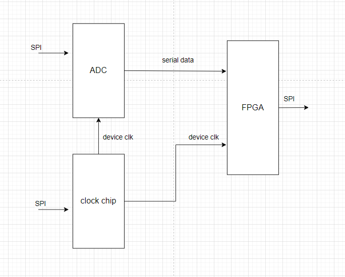
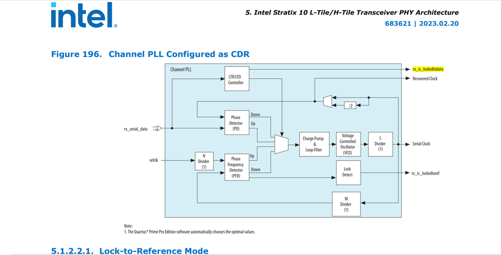
My device version is stratix10 1SX110HN2F43I2VG. I use FPGA to receive JESD204B data from ADC chip. When I power up the PCB, both the FPGA and ADC do not have device clock input, or the input is at a lower erroneous frequency.Then I configure the clock chip through SPI so that both the ADC and FPGA receive the correct device clock. However, the ADC still does not output JESD204B data. Then, I configure the ADC through SPI to output JESD204B data. I found that the rx_islockedtodata signal is 0. I tried disconnecting the xcvr_reset_control IP core, manually resetting rx_analogreset and rx_digitalreset, but still could not make rx_islockedtodata high. After reconnecting the xcvr_reset_control IP core and reloading the sof file, rx_islockedtodata successfully becomes 0xF. This means that even though the FPGA has received the 204B data rx_islockedtodata remains at 0. After reloading the sof file again, rx_islockedtodata becomes 0xF. How can I bring the rx_islockedtodata signal high without reloading the sof file? Or what variables during the process of reloading the sof file cause the rx_islockedtodata signal to go high? Does the FPGA only program sof file when ensuring JESD204B data input?
thanks
- Tags:
- JESD204B
- Mark as New
- Bookmark
- Subscribe
- Mute
- Subscribe to RSS Feed
- Permalink
- Report Inappropriate Content
Hi,
Yes the root cause is same as you mentioned - no ref clock when FPGA is configured (First time).
Can you please share the reason for configuring LMK04832 via SPI for every power cycle?
Can you program the LMK04832 once and it'll retain the clock configuration? -> If yes Do it.
If not, other solutions:
- Program the FPGA via jic and rbf -> So that even after power cycle FPGA will have its configuration and you just need to give a reset command to FPGA and it'll work. Power up-> FPGA program the clk chip via SPI -> Reset command for FPGA.
- You can implement BMC (Board Management Controller) in your design. BMC will configure the LMK chip first and then bring up the FPGA.
Regards,
HarshX
Link Copied
- Mark as New
- Bookmark
- Subscribe
- Mute
- Subscribe to RSS Feed
- Permalink
- Report Inappropriate Content
- Mark as New
- Bookmark
- Subscribe
- Mute
- Subscribe to RSS Feed
- Permalink
- Report Inappropriate Content
- Mark as New
- Bookmark
- Subscribe
- Mute
- Subscribe to RSS Feed
- Permalink
- Report Inappropriate Content
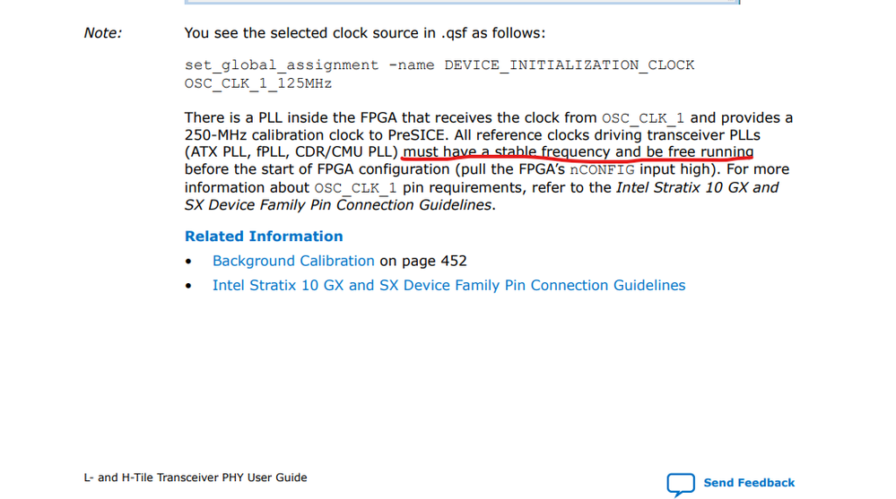
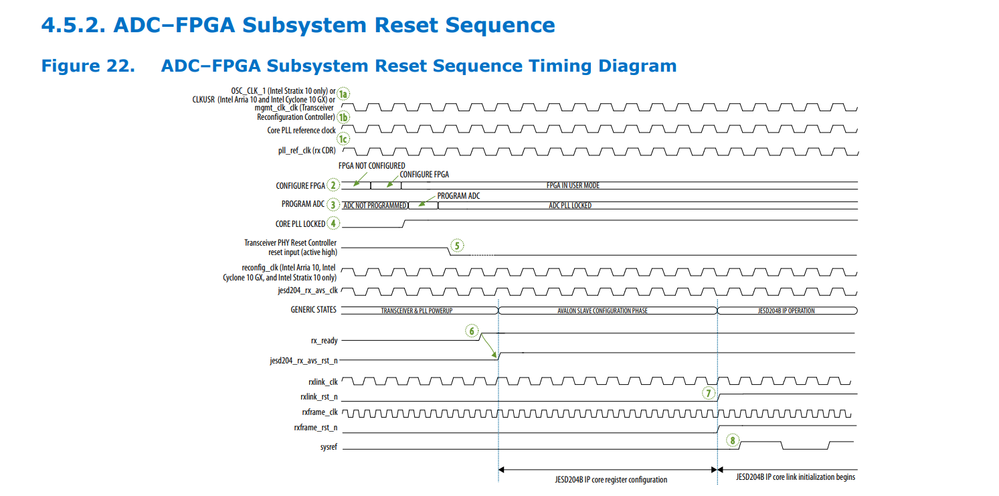
I noticed the reset sequence in the datasheet, which states that before programming the FPGA, stable OSC_CLK_1, management clock, and transceiver reference clock (device clk) are required. However, for my current design, after powering up the board, only OSC_CLK_1 and the management clock are stable. The device clk comes from the clock chip, which needs to be generated through FPGA configuration after I finish configuring the FPGA. I attempted to program the FPGA for the first time and then use the FPGA to configure the clock chip via SPI. At this point, I have stable OSC_CLK_1, management clock, and transceiver reference clock (device clk). Then, I program the FPGA again and configure the ADC via FPGA using SPI to output JESD204B data. rx_islockedtodata can become F, and data reception works properly. Can I achieve JESD204B data reception with only one FPGA programming? Could ADM experts or technical support give some advice? thanks.
- Mark as New
- Bookmark
- Subscribe
- Mute
- Subscribe to RSS Feed
- Permalink
- Report Inappropriate Content
Hi,
Thanks for contacting Intel.
I'm assigned to support request.
I'll investigate on this case.
Can you please share the following details:
- Quartus version you are using.
- Which Clock Chip you are using (as mentioned in your block diagram) -> This is just to figure out is there any default clock setting? if you program the clock and power cycle the board is it able to retain the settings?
Thanks for your patience.
Best regards,
HarshX
- Mark as New
- Bookmark
- Subscribe
- Mute
- Subscribe to RSS Feed
- Permalink
- Report Inappropriate Content
Hi
I am using quartus Pro 22.3 , clock chip is LMK04832 , according to my latest findings, before configuring the FPGA, the transceiver must has a stable reference clock. before loading the .sof file for the first time, the clock chip was not configured, leaving the transceiver without a reference clock. After loading the .sof file, the FPGA automatically configured the clock chip, then the clock chip consistently provided stable output. Therefore, by the time I load the .sof file for the second time, the transceiver already had a stable reference clock, and rx_islockedtodata change to high.I'm not entirely sure if this is the root cause of the issue

- Mark as New
- Bookmark
- Subscribe
- Mute
- Subscribe to RSS Feed
- Permalink
- Report Inappropriate Content
Hi,
Yes the root cause is same as you mentioned - no ref clock when FPGA is configured (First time).
Can you please share the reason for configuring LMK04832 via SPI for every power cycle?
Can you program the LMK04832 once and it'll retain the clock configuration? -> If yes Do it.
If not, other solutions:
- Program the FPGA via jic and rbf -> So that even after power cycle FPGA will have its configuration and you just need to give a reset command to FPGA and it'll work. Power up-> FPGA program the clk chip via SPI -> Reset command for FPGA.
- You can implement BMC (Board Management Controller) in your design. BMC will configure the LMK chip first and then bring up the FPGA.
Regards,
HarshX
- Mark as New
- Bookmark
- Subscribe
- Mute
- Subscribe to RSS Feed
- Permalink
- Report Inappropriate Content
Hi,
Thank you for your response , how can I make a reset command for FPGA after LMK04832 configuration complete?
- Mark as New
- Bookmark
- Subscribe
- Mute
- Subscribe to RSS Feed
- Permalink
- Report Inappropriate Content
Hi,
I hope you do have main reset signal in your design, use that (Here I'm guessing that resetting only the JESD204B is not working).
About how you can change the values/variables once the FPGA is programmed ->SYSTEM DEBUGGING TOOLS -> you can use ISSP (In-System Sources and Probes), you have to implement this in your design beforehand. By using Intel System Console GUI you can give command to make changes in your design (enabling reset, changing values, etc) on run.
ISSP: 1.3.1. In-System Sources and Probes (intel.com)
System Console: 7.1. Introduction to System Console (intel.com)
Kindly also answer queries in previous comments.
I hope this info is useful.
Regards,
HarshX
- Mark as New
- Bookmark
- Subscribe
- Mute
- Subscribe to RSS Feed
- Permalink
- Report Inappropriate Content
I attempted to manually control rx_analogreset and rx_digitalreset of the jesd204b IP core through ISSP, affter LMK04832 is configured , but it didn't work. It seems that configuring LMK04832 before FPGA is the only solution.
- Mark as New
- Bookmark
- Subscribe
- Mute
- Subscribe to RSS Feed
- Permalink
- Report Inappropriate Content
Hi,
Kindly follow reset scheme: 4.5. Reset Scheme (intel.com)
Can you please share the reason for configuring LMK04832 via SPI for every power cycle?
Why not separately program the clock chip once so after every power cycle clk chip will have the same configuration which is needed by FPGA? (LMK03328 EVM Setup and Programming with TICS Pro GUI | Video | TI.com).
Regards,
HarshX
- Mark as New
- Bookmark
- Subscribe
- Mute
- Subscribe to RSS Feed
- Permalink
- Report Inappropriate Content
Thank you. We didn't notice this when designing the clock scheme for the project initially. It should be more reasonable to configure the clock chip in another way. The changes will be implemented in the next version of the PCB.
- Subscribe to RSS Feed
- Mark Topic as New
- Mark Topic as Read
- Float this Topic for Current User
- Bookmark
- Subscribe
- Printer Friendly Page


