- Mark as New
- Bookmark
- Subscribe
- Mute
- Subscribe to RSS Feed
- Permalink
- Report Inappropriate Content
Hi all,
I want to first start by saying a massive thanks to Rysc for putting out this TimeQuest guide: http://alteraforums.net/forum/showthread.php?t=25676&highlight=guide Unfortunately due to being very short of time I have pretty much just read the first 30-odd pages (the getting started section) and am struggling slightly already... I am trying to properly constrain my design, but I am not used to working with FPGA's so am finding Quartus II, ModelSim, TimeQuest etc a lot to take in just to design and compile a working design... however I am trying to persevere. The main thing I am struggling with is Rysc's Step 5 from the getting started, i.e. Modify the -max and -min delays to account for external delays. I was trying to use an iterative approach, and even with the max and min input and output delays set as 0.0 for the time being, the majority of paths find this acceptable. The only timing problems I have seem to be coming from the output of my PLL. (The output from my PLL is basically 4x the speed of my LVDS clock) Did I need to define my generated clock specifically or does using "derive_pll_clocks" suffice? I've attached a screenshot of setup Report Timing for the PLL output. If anyone can help and save me hours of staring blankly at user guides and tutorials until the penny drops, then it is much appreciated!! Cheers, Lee H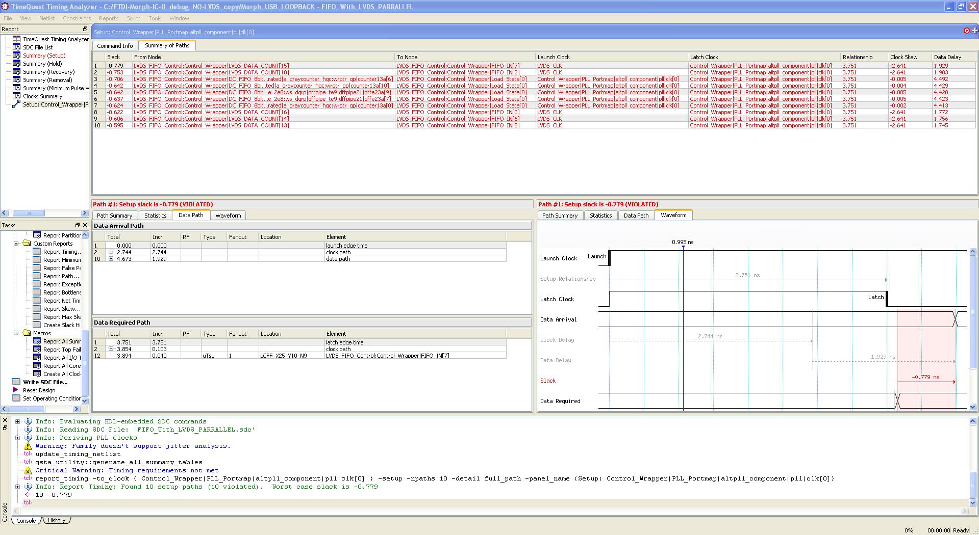
Link Copied
- Mark as New
- Bookmark
- Subscribe
- Mute
- Subscribe to RSS Feed
- Permalink
- Report Inappropriate Content
Is this an I/O port? Looking at the Data Path tab, I'd guess it's internal to the FPGA.
Your transfer is from rising edge to falling edge(i.e. the latching logic triggers on the falling edge), so it defaults to a half-cycle setup relationship, or 3.75ns. Your latch clock is on a PLL, which basically removes the clock tree delay, but your source clock is not. So the clock skew completely cuts into your setup requirement. Your data path delay is less than 2ns, but because of these two things it's still not enough. Is the 3.75ns requirement your intended transfer? If so, can the data path be shorter? I doubt it can be 800ps shorter, but might be. Can you change the clocks to make the requirement/skew more palatable? Reading the document will help with understanding, but won't provide a solution, since this is unique to your design.- Mark as New
- Bookmark
- Subscribe
- Mute
- Subscribe to RSS Feed
- Permalink
- Report Inappropriate Content
--- Quote Start --- Is this an I/O port? Looking at the Data Path tab, I'd guess it's internal to the FPGA. Your transfer is from rising edge to falling edge(i.e. the latching logic triggers on the falling edge), so it defaults to a half-cycle setup relationship, or 3.75ns. Your latch clock is on a PLL, which basically removes the clock tree delay, but your source clock is not. So the clock skew completely cuts into your setup requirement. Your data path delay is less than 2ns, but because of these two things it's still not enough. Is the 3.75ns requirement your intended transfer? If so, can the data path be shorter? I doubt it can be 800ps shorter, but might be. Can you change the clocks to make the requirement/skew more palatable? Reading the document will help with understanding, but won't provide a solution, since this is unique to your design. --- Quote End --- Hi Rysc and thanks for your reply. Here's a little bit more info about what I am trying to achieve! Basically my design is to be used in some simple DV testing, where I am taking the top and bottom line of a screen from a LVDS stream and sending it them out over usb. The LVDS data is deserialised by a deserialiser board into parallel 24-bit LVDS and a Pixel Clock. For the moment instead of using the actual LVDS RGB565 data, I am just using an 18 bit counter (so I know what my expected data is for simulation and can see which bytes im losing/gaining when debugging). Aswell as these 18 bits, there are 4 reserved channels a Hsync and a Vsync. I am using the actual pixel clock Hsync and Vsync that are generated internally. The data is clocked into the FPGA using a 33.3MHz clock (LVDS_CLK in my design) this clock is fed through a PLL to give a clock four times the speed (this is MULT_CLK in my design). So that my 24-bit LVDS data can be clocked into an 8 bit DC fifo. The clock is four times the speed so that the 3 data bytes can be written, and FIFO_WR can be held low on the rising edge of LVDS_CLK to avoid any race conditions or problems clocking bytes into the FIFO. The data is now clocked into the FIFO on the RISING edge of the MULT_CLK, which got rid of the timing issues shown in the screenshot attached to my last message. My design simulates correctly, and now, timequest gives no errors about timing. However I MUST have timing issues somewhere as the data I am recieving over USB has missing data bytes and bytes read more than once. I am using the Morph-IC-II board which has the Cyclone II FPGA, and an FTDI FT2232H chip to handle the USB side of things. Once an entire line of pixels (800 pixels => 2400 Bytes) has been clocked into the FIFO on the FPGA, then it is clocked out to the TX buffer on the FT2232 chip. This then waits for a command on a little C# application which allows it to transmit the contents of its TX buffer over USB. All buffer sizes are larger than they need to be, so I am not losing data there... so there must be a timing issue somewhere... but I can't find it and don't know where to begin as the simulation looks fine, timequest seems happy, but it doesn't work when dropped onto the hardware... Any help or ideas are much appreciated as I am very stuck and a little out of my depth!!! Anymore information that is required just shout!! Regards, Lee H
- Mark as New
- Bookmark
- Subscribe
- Mute
- Subscribe to RSS Feed
- Permalink
- Report Inappropriate Content
Well TimeQuest may seem happy, but I am still getting timing errors somewhere...
My design simulates in ModelSim, I am not getting any errors from TimeQuest but I feel like I am still getting some timing errors in the actual implimentation on hardware as I am loosing some data bytes, and getting repeated reads of other data bytes within my log files, and I am struggling to work out where in my design they are coming from. I have a dual clocked FIFO, to which I am trying to write 1 line of 800 24-bit pixels (2400 bytes) using my LVDS_CLK, and the data should be clocked out of the FIFO using the FTDI_CLK. As I am using the Morph-IC-II Board the FT_CLK is provided by the FT2232H USB Bridge chip. When the data is clocked out of the FIFO in the FPGA it should be clocked into the TX FIFO on the FT2232H, which will await a command which it recieved over USB before transmitting it to the application. I am struggling to find where my data is getting mangled but think its probably due to timings somewhere within the FPGA... but am struggling to get any further as I dont have any Unconstrained paths, or things failing setup or hold...so being new to this I am kind of at a loss.... Any help on this is greatly appreciated. Regards, Lee H- Mark as New
- Bookmark
- Subscribe
- Mute
- Subscribe to RSS Feed
- Permalink
- Report Inappropriate Content
Use SignalTap. It's getting down and dirty, but it should always lead to the problem.
First place to look is probably the FIFO. Does your logic monitor the full/empty flags? They can be squirrelly, and if the logic doesn't adjust, that's the type of thing that leads to extra/missing bytes. Just a thought. I doubt this is something that can be figured out over the forum.- Mark as New
- Bookmark
- Subscribe
- Mute
- Subscribe to RSS Feed
- Permalink
- Report Inappropriate Content
Cheers for the help an advice... unfortunately I have no byteblaster or other JTAG type device in order to use Signal Tap, as with the Morph board you program the FPGA over the USB interface... :(
I am only ever reading in 2400 bytes at a time then there are large gaps either side, as I read the first and final line of a frame, then stop reading anything into the fifo using a flag that signals the end of the first frame. The fifo is 4096 bytes long, so I shouldn't be losing data there, and the TX BUFFER in the FT2232 is defaulted to 4KB but I have it set to its maximum of 64KB, so I wont be trying to write to a full buffer there or anything either! Also, with respect to the FIFO Flags, my logic ensures that I stop reading from it when its empty, and can't write to it if its full.... its the fact that I am getting some double reads of data and stuff that is confusing the hell out of me... and as I have only just graduated and jumped into this with both feet; I am kinda feeling that I don't quite have the knowledge or the tools to crack this nut just yet! I have a feeling it is something that can't really be solved over the forum, there was just the hope, that someone may suggest something that would seem obvious to check to them, but that I may not have even considered due to my lack of experience with FPGA's Once again, cheers for your help and your TimeQuest guide... and I am sure you'll hear a eureka on the forums if i crack it! Regards, Lee H- Mark as New
- Bookmark
- Subscribe
- Mute
- Subscribe to RSS Feed
- Permalink
- Report Inappropriate Content
it may not be right to blame timing on fifo rate problems. Since you lose some data and repeat others, it points more to flow control and possibly fifo being working close to full/empty points. one issue with fifos is when it gets full it may need emptying by reset as it hits near full point and never recovers.
- Mark as New
- Bookmark
- Subscribe
- Mute
- Subscribe to RSS Feed
- Permalink
- Report Inappropriate Content
--- Quote Start --- it may not be right to blame timing on fifo rate problems. Since you lose some data and repeat others, it points more to flow control and possibly fifo being working close to full/empty points. one issue with fifos is when it gets full it may need emptying by reset as it hits near full point and never recovers. --- Quote End --- My FIFO is bigger than required for my design, which should ensure that I get no full points, and my logic also looks for the FIFO_FULL flag and will not write to the fifo if it is full.... also once the fifo is filled as with 1 line of data (2400 words of 8 bits each, in a buffer 8 bits wide, and 4069 words long) the data is clocked out until the buffer is empty. So I don't really think that there should be any problems with the fifo with respect to writing to it when its full, or reading from it when it's empty. I am trying to read the data in on the rising edge of my MULT_CLK, which is 4x faster than my LVDS_CLK. These clks are synchronised as LVDS_CLK is used to generate MULT_CLK using a PLL. I have 3 cycles where a byte of data is clocked into the FIFO, and one rising edge of MULT_CLK where a byte is not clocked in (to avoid any race conditions when the next 24bit word is loaded into the FPGA using the LVDS_CLK). I have tried to use the mutlicycle function in TimeQuest to ensure that the correct edge of the latch clock is constrained for the corresponding paths for setup. However, when using multicycle to constrain the hold times, rather than my launch and latch clock occuring at 0ns it they occur 1 period of the slower launch clock later. Is this what I should be expecting? As the launch for setup occurs at 0ns but the launch for hold occurs at 30.011... Regards, Lee H
- Mark as New
- Bookmark
- Subscribe
- Mute
- Subscribe to RSS Feed
- Permalink
- Report Inappropriate Content
Hi all,
I managed to constrain pretty much all of my timing problems... and have gotten rid of all sporadic/intermittent problems with missing and extra bytes. I now have only a periodic problem, where after every 510 bytes which are successfully recieved I loose 2 bytes of data that I should recieve. Although my logic simulates properly using ModelSim I believe this is probably something within my design rather than anything else. However to track down at which point this occurs I want to test my FT245 synchronous interface and my DC FIFO reads and writes individually to try to find the weak link in the chain. I DO NOT HAVE ACCESS TO SIGNAL TAP (basically as my device is programmed over USB and I have no suitable JTAG connector to allow me to use signal tap) However I am trying to re-create small sections of my design with dummy data to test each part individually to track down the fault. However, when trying to impliment my FT245 Synchronous interface I am failing to meet my timing requirements. The table below shows the timing requirements of the 245 interface, with the timing diagrams shown in the first attachment. name ..|.. min ..|.. nom ..|.. max ..|.. units ..|.. comment ---------|--------|----------|----------|----------|------------- t1 .......|...........|..16.67..|.............|.. ns .....|.. CLKOUT period t2 .......|...7.5...|.. 8.33 ..|.............|.. ns .....|.. CLKOUT high period t3 .......|...7.5...|.. 8.33 ..|.............|.. ns .....|.. CLKOUT low period t4 .......|...1......|.. 7.15 ..|.............|.. ns .....|.. CLKOUT to RXF# t5 .......|...1......|.. 7.15 ..|.............|.. ns .....|..CLKOUT to read DATA valid t6 .......|...1......|.. 7.15 ..|.............|.. ns .....|..OE# to read DATA valid t7 .......|...1......|.. 7.15 ..|.............|.. ns .....|..CLKOUT to OE# t8 .......|...11....|............|.............|.. ns .....|..RD# setup time t9 .......|...0......|............|.............|.. ns .....|..RD# hold time t10 .....|...1......|.. 7.15 ..|.............|.. ns .....|..CLKOUT TO TXE# t11 .....|...11....|............|.............|.. ns .....|..Write DATA setup time t12 .....|...0......|............|.............|.. ns .....|..Write DATA hold time t13 .....|...11....|............|.............|.. ns .....|..WR# setup time t14 .....|...0......|............|.............|.. ns .....|..WR# hold time I am still struggling to understand how the setup and hold times are manipulated using the set_input_delay and set_output_delay. Would:
set_output_delay -clock FTDI_CLK_ext -max 11.0 ]
set_output_delay -clock FTDI_CLK_ext -min 0.0 ]
Be correct to constrain AC[3] (which is the WR# signal) so that its setup time is at minimum 11ns and its hold 0ns... or am I completely missing the point. Also if you set a constraint and timequest fails. You recompile your design so that it can be refit. If the clock and data delays are still too long to meet your timing requirements how do you proceed further after this? Sorry for being so rubbish with this! Any and all help much appreciated!! Regards, Lee H
- Mark as New
- Bookmark
- Subscribe
- Mute
- Subscribe to RSS Feed
- Permalink
- Report Inappropriate Content
--- Quote Start ---
set_output_delay -clock FTDI_CLK_ext -max 11.0 ]
set_output_delay -clock FTDI_CLK_ext -min 0.0 ]
Be correct to constrain AC[3] (which is the WR# signal) so that its setup time is at minimum 11ns and its hold 0ns... or am I completely missing the point. Also if you set a constraint and timequest fails. You recompile your design so that it can be refit. If the clock and data delays are still too long to meet your timing requirements how do you proceed further after this? --- Quote End --- The timing constraints are OK, I assume that FTDI_CLK_ext is supplied by the FT245 chip. If after recompiling the timing fails, you have to inspect the failing paths using the report-timing function in TimeQuest itself. Look through the datapath to find out where the bottleneck(s) are. Now with 60MHz and 11 ns setup time you almost have to register anything going to the FT245 chip and very likely use IO-registers.
- Mark as New
- Bookmark
- Subscribe
- Mute
- Subscribe to RSS Feed
- Permalink
- Report Inappropriate Content
Hi josyb,
Thanks for your response. FTDI_CLK is supplied by the FT245 chip, but FTDI_CLK_ext is a virtual clock to represent the latch clock as this is what is suggested in Rysc's TimeQuest guide. That is the problem I have been finding, with only a 16.67ns clock period and a requirement for an 11ns setup time, timing has been failing as I only have 5.67ns in which to accomodate both the clock delay and the data delay. I know how to instantiate a register normally, but not how to use the input and output registers that are already connected to an IO pin. The timing report for the failing pins is shown in the attachment. The biggest bottlenecks all appear to be the actual IO pin itself with about a 3ns delay being created there... Once again, thanks for your time, Regards, Lee H
- Mark as New
- Bookmark
- Subscribe
- Mute
- Subscribe to RSS Feed
- Permalink
- Report Inappropriate Content
Lee,
Am I right that you are in fact using a FT232 chip but then in FT245 synchronous style? I had to search a bit before I found that application note. One way to go is to make sure that the IO data for output is registered, e.g. being the registered output of a FIFO. Another way is to add a register to everything that goes to the FT-chip. This will meet timing. But not function as you now may write when the FT-chip signals full. The idea is that you now recognize such a 'MISSED_WRITE' and modify your writing state machine to cope with that and re-submit that not-written data when the flag goes inactive again. BTW you don't have to declare a virtual clock, you can use the incoming clock to specify the output delays. Good luck! Josy- Mark as New
- Bookmark
- Subscribe
- Mute
- Subscribe to RSS Feed
- Permalink
- Report Inappropriate Content
Yes, sorry it is the FT2232H chip functioning in FT245 synchronous interface mode, as I am using the FTDI Morph-IC-II board which has a Cyclone II FPGA on it.
I will try sending all outputs through registers to try to sort out timing. Cheers, Lee H- Mark as New
- Bookmark
- Subscribe
- Mute
- Subscribe to RSS Feed
- Permalink
- Report Inappropriate Content
Hiya, I am struggling with this a little.
even putting a register before my outputs doesn't seem to work, as the 3ns delay appears to be across the tristate buffer for the IO pin. As I need the pin to be an IO pin is there another way to make it meet the 11ns setup time requirement? or do I need to look into multicycling and rather than having my latch clock on the next rising edge of the latch clock, have it on the rising edge after that? with registers, here is my timing, and the locations of the paths within the RTL viewer. I don't really know how FTDI expect you to be able to meet the 11ns setup with a clock period of 16.67ns and the typical data and clock delays that I am recieving!? Reagrds, Lee H- Mark as New
- Bookmark
- Subscribe
- Mute
- Subscribe to RSS Feed
- Permalink
- Report Inappropriate Content
Lee,
you have to 'promote' the register to be an IO-register. It is not the tri-state function adding the delay but the path from an internal register over the IO-buffer to the pin. You can use the assignment editor to do this: From | To | AssignementName | Value | Enabled <empty> | AD | Fast Output regsiter | On | Yes I had the same issue with Cypress' CY7C69013 FX2 USB controller- Mark as New
- Bookmark
- Subscribe
- Mute
- Subscribe to RSS Feed
- Permalink
- Report Inappropriate Content
I had the same problem with those hideous setup-times of FT2232, even with forcing the register to be in the I/O-pad. The clock-delay is too long if you route the incoming clock to the registers.
I had to recreate an 1:1 copy of the incoming USB clock with a PLL in Normal compensation mode. This automatically shifts the PLL outclock to compensate for the bulk of the delay in the clocktree. After this, you still have no time to do any logic, but all inputs and outputs from the FT2232 have to be registered. Yes, inputs too - the FT2232 has up to 7.15 ns delay in the fifo signals RXF and TXE leaving little margin inside the FPGA for anything except a register. I'm still struggling with the write-state machine though, where I have to monitor the external fifo-full signal (TXF), which is registred and thus delayed 1 cycle, to see if a write "didn't take". Unfortunately it's not very simple, as by the time you detect this, you will have acked *two* bytes from the fifo in the FPGA, leaving you to juggle around up to two bytes (one if the internal FIFO got empty), causing a real MESS when trying to resend them :/ You could conceivably even run into the situation where bytes are read out-of-order by the FT2232. If anybody has any ideas: writes occurs through pin-based FPGA-registers data_out_r and wr_n_r, and the FT2232 fifo-full is from the registred input txe_n_r. If we have data to write, and load 0 in wr_n_r and data in data_out_r, the cycle it shows on the output the FT2232 might inactivate txe_n. We won't see this until the cycle after, when we need to have yet another byte out on the bus to get the full throughput. So at that point, we have the byte we lost completely, and we have the byte currently on the data_out_r. I tried adding another register that keeps the last byte from data_out_r. But then I got into the mess with trying to resend them both after txe_n_r activates again in a clean way preferably not going into a special state where they are both completely transmitted before starting reading from the internal FIFO. I don't know if the FT2232 is designed so it can end up in a state toggling txe for every byte, which would cause a huge loss in performance with the above solution :/ Huaarhh.- Mark as New
- Bookmark
- Subscribe
- Mute
- Subscribe to RSS Feed
- Permalink
- Report Inappropriate Content
Hi Exolon,
I spoke to FTDI a while ago when I was having problems with my design, and they sent me a revised, relaxed set of timing constraints which they assured me work (and they seem fine to me) which helps a little... I have attached the document they sent. Also I managed to avoid your problems as my design was quite a simple one. Basically as I was using the FT245 synchronous mode, no matter what you set the TX and RX buffer sizes to on the FT2232H, they are only 512 Bytes as that's the maximum packet size in USB Bulk mode. I was multiplexing 24bit words into my 8 bit output buffer, so I just filled the TX buffer with 510 bytes, and stopped writing to the buffer. Which meant I never needed to look for the TXF flag, and once my application had finished reading the buffer, so that it was empty again, the application sent a byte to trigger my next packet of data to be loaded into the FT2232's TX buffer.... It's not the most elegant solution, and probably not what you are looking for, but for my simple design it seems to have worked well enough...- Mark as New
- Bookmark
- Subscribe
- Mute
- Subscribe to RSS Feed
- Permalink
- Report Inappropriate Content
Thats funny, I'm also multiplexing 24-bit words into the 8-bit USB bus :)
Anyway, thanks for the FTDI-document - seems like they relaxed the 11 ns setup times to 8 ns. This will surely give me some nice slack. I can't take the easy route like you did with ignoring TXE since I have huge data-buffers to send continously more or less. Though, this morning I managed to get timing closure and good function of my interface even with the 11 ns timing. The resulting speed (writing from Cyclone-3 to FTDI2232H and reading from a Linux PC up to a user-mode program using libusb) was a whopping 43 mbyte/s! Satisfying! And it seems it works without glitches (yet). As a side-effect I learned a lot of SDC as well :)- Subscribe to RSS Feed
- Mark Topic as New
- Mark Topic as Read
- Float this Topic for Current User
- Bookmark
- Subscribe
- Printer Friendly Page